Instrukcja obsługi Supermicro A2SDV-12C+-TLN5F
Supermicro
płyta główna
A2SDV-12C+-TLN5F
Przeczytaj poniżej 📖 instrukcję obsługi w języku polskim dla Supermicro A2SDV-12C+-TLN5F (111 stron) w kategorii płyta główna. Ta instrukcja była pomocna dla 2 osób i została oceniona przez 2 użytkowników na średnio 4.5 gwiazdek
Strona 1/111
![](https://manualstech.ams3.cdn.digitaloceanspaces.com/html/nl/supermicro/a2sdv-12c-plus-tln5f/html/bg1.png)
USER MANUAL
Revision 1.0
A2SDV-8C-TLN5F
A2SDV-12C+-TLN5F
A2SDV-16C-TLN5F
![](https://manualstech.ams3.cdn.digitaloceanspaces.com/html/nl/supermicro/a2sdv-12c-plus-tln5f/html/bg2.png)
The information in this user’s manual has been carefully reviewed and is believed to be accurate. The vendor assumes
no responsibility for any inaccuracies that may be contained in this document, and makes no commitment to update
or to keep current the information in this manual, or to notify any person or organization of the updates. Please Note:
For the most up-to-date version of this manual, please see our website at www.supermicro.com.
Super Micro Computer, Inc. ("Supermicro") reserves the right to make changes to the product described in this manual
at any time and without notice. This product, including software and documentation, is the property of Supermicro and/
or its licensors, and is supplied only under a license. Any use or reproduction of this product is not allowed, except
as expressly permitted by the terms of said license.
IN NO EVENT WILL Super Micro Computer, Inc. BE LIABLE FOR DIRECT, INDIRECT, SPECIAL, INCIDENTAL,
SPECULATIVE OR CONSEQUENTIAL DAMAGES ARISING FROM THE USE OR INABILITY TO USE THIS PRODUCT
OR DOCUMENTATION, EVEN IF ADVISED OF THE POSSIBILITY OF SUCH DAMAGES. IN PARTICULAR, SUPER
MICRO COMPUTER, INC. SHALL NOT HAVE LIABILITY FOR ANY HARDWARE, SOFTWARE, OR DATA STORED
OR USED WITH THE PRODUCT, INCLUDING THE COSTS OF REPAIRING, REPLACING, INTEGRATING,
INSTALLING OR RECOVERING SUCH HARDWARE, SOFTWARE, OR DATA.
Any disputes arising between manufacturer and customer shall be governed by the laws of Santa Clara County in the
State of California, USA. The State of California, County of Santa Clara shall be the exclusive venue for the resolution
of any such disputes. Supermicro's total liability for all claims will not exceed the price paid for the hardware product.
FCC Statement: This equipment has been tested and found to comply with the limits for a Class A digital device
pursuant to Part 15 of the FCC Rules. These limits are designed to provide reasonable protection against harmful
interference when the equipment is operated in a commercial environment. This equipment generates, uses, and can
radiate radio frequency energy and, if not installed and used in accordance with the manufacturer’s instruction manual,
may cause harmful interference with radio communications. Operation of this equipment in a residential area is likely
to cause harmful interference, in which case you will be required to correct the interference at your own expense.
California Best Management Practices Regulations for Perchlorate Materials: This Perchlorate warning applies only
to products containing CR (Manganese Dioxide) Lithium coin cells. “Perchlorate Material-special handling may apply.
See ”.www.dtsc.ca.gov/hazardouswaste/perchlorate
WARNING: Handling of lead solder materials used in this product may expose you to lead, a
chemical known to the State of California to cause birth defects and other reproductive harm.
The products sold by Supermicro are not intended for and will not be used in life support systems, medical equipment,
nuclear facilities or systems, aircraft, aircraft devices, aircraft/emergency communication devices or other critical
systems whose failure to perform be reasonably expected to result in signicant injury or loss of life or catastrophic
property damage. Accordingly, Supermicro disclaims any and all liability, and should buyer use or sell such products
for use in such ultra-hazardous applications, it does so entirely at its own risk. Furthermore, buyer agrees to fully
indemnify, defend and hold Supermicro harmless for and against any and all claims, demands, actions, litigation, and
proceedings of any kind arising out of or related to such ultra-hazardous use or sale.
Manual Revision: 1.0
Release Date: February 14, 2018
Unless you request and receive written permission from Super Micro Computer, Inc., you may not copy any part of this
document. Information in this document is subject to change without notice. Other products and companies referred
to herein are trademarks or registered trademarks of their respective companies or mark holders.
Copyright © 2018 by Super Micro Computer, Inc.
All rights reserved.
Printed in the United States of America
![](https://manualstech.ams3.cdn.digitaloceanspaces.com/html/nl/supermicro/a2sdv-12c-plus-tln5f/html/bg3.png)
3
Note: Additional Information given to differentiate various models or to provide in-
formation for correct system setup.
Preface
Preface
About This Manual
This manual is written for system integrators, IT technicians and knowledgeable end users.
It provides information for the installation and use of the A2SDV-8C/-12C+/-16C-TLN5F
motherboard.
About This Motherboard
The Supermicro A2SDV-8C/-12C+/-16C-TLN5F motherboard comes with an integrated Intel®
Atom SoC (FCBGA1310) supporting up to 16 Cores, a TDP of 32W and is optimized for
low-power consumption. This is a small form factor motherboard that is optimized for the
embedded solution. The following are some features that are offered: two M.2 connectors (one
M-Key and one B-Key), four 10G LAN ports, PCI-E 3.0 x8 expandability either via expansion
slot#6 OR #7, and the reliability and dependability of a Supermicro product. Please note that
this motherboard is intended to be installed and serviced by professional technicians only.
For processor/memory updates, please refer to our website at http://www.supermicro.com/
products/.
Conventions Used in the Manual
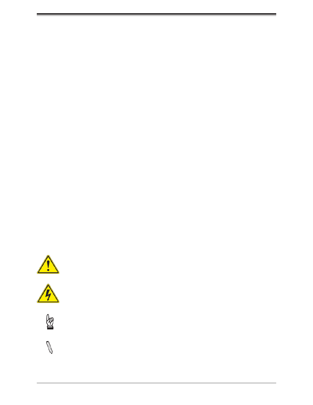
Special attention should be given to the following symbols for proper installation and to prevent
damage done to the components or injury to yourself:
Warning! Indicates high voltage may be encountered when performing a procedure.
Warning! Indicates important information given to prevent equipment/property damage
or personal injury.
Important: Important information given to ensure proper system installation or to
relay safety precautions.
![](https://manualstech.ams3.cdn.digitaloceanspaces.com/html/nl/supermicro/a2sdv-12c-plus-tln5f/html/bg4.png)
4
Contacting Supermicro
Headquarters
Address: Super Micro Computer, Inc.
980 Rock Ave.
San Jose, CA 95131 U.S.A.
Tel: +1 (408) 503-8000
Fax: +1 (408) 503-8008
Email: marketing@supermicro.com (General Information)
support@supermicro.com (Technical Support)
Website: www.supermicro.com
Europe
Address: Super Micro Computer B.V.
Het Sterrenbeeld 28, 5215 ML
's-Hertogenbosch, The Netherlands
Tel: +31 (0) 73-6400390
Fax: +31 (0) 73-6416525
Email: sales@supermicro.nl (General Information)
support@supermicro.nl (Technical Support)
rma@supermicro.nl (Customer Support)
Website: www.supermicro.nl
Asia-Pacic
Address: Super Micro Computer, Inc.
3F, No. 150, Jian 1st Rd.
Zhonghe Dist., New Taipei City 235
Taiwan (R.O.C)
Tel: +886-(2) 8226-3990
Fax: +886-(2) 8226-3992
Email: support@supermicro.com.tw
Website: www.supermicro.com.tw
A2SDV-8C/-12C+/-16C-TLN5F User's Manual
![](https://manualstech.ams3.cdn.digitaloceanspaces.com/html/nl/supermicro/a2sdv-12c-plus-tln5f/html/bg5.png)
5
Table of Contents
Chapter 1 Introduction
1.1 Checklist ...............................................................................................................................8
Quick Reference ...............................................................................................................11
Quick Reference Table ......................................................................................................12
Motherboard Features .......................................................................................................14
1.2 Processor Overview ...........................................................................................................17
1.3 Special Features ................................................................................................................17
Recovery from AC Power Loss .........................................................................................17
1.4 System Health Monitoring ..................................................................................................17
Onboard Voltage Monitors ................................................................................................18
Fan Status Monitor with Firmware Control .......................................................................18
Environmental Temperature Control .................................................................................18
System Resource Alert......................................................................................................18
1.5 ACPI Features ....................................................................................................................18
1.6 Power Supply .....................................................................................................................19
1.7 Serial Port ...........................................................................................................................19
Chapter 2 Installation
2.1 Static-Sensitive Devices .....................................................................................................20
Precautions .......................................................................................................................20
Unpacking .........................................................................................................................20
2.2 Motherboard Installation .....................................................................................................21
Tools Needed ....................................................................................................................21
Location of Mounting Holes ..............................................................................................21
Installing the Motherboard.................................................................................................22
2.3 Memory Support and Installation .......................................................................................23
Memory Support ................................................................................................................23
DIMM Module Population Conguration ...........................................................................23
DIMM Module Population Sequence ................................................................................24
DIMM Installation ..............................................................................................................25
DIMM Removal .................................................................................................................25
2.4 Rear I/O Ports ....................................................................................................................26
Preface
![](https://manualstech.ams3.cdn.digitaloceanspaces.com/html/nl/supermicro/a2sdv-12c-plus-tln5f/html/bg6.png)
6
2.5 Front Control Panel ............................................................................................................31
2.6 Connectors .........................................................................................................................36
Power Connections ...........................................................................................................36
Headers .............................................................................................................................38
2.7 Jumper Settings .................................................................................................................45
How Jumpers Work ...........................................................................................................45
2.8 LED Indicators ....................................................................................................................51
Chapter 3 Troubleshooting
3.1 Troubleshooting Procedures ..............................................................................................53
Before Power On ..............................................................................................................53
No Power ..........................................................................................................................53
No Video ...........................................................................................................................53
System Boot Failure ..........................................................................................................54
Memory Errors ..................................................................................................................54
Losing the System's Setup Conguration .........................................................................55
When the System Becomes Unstable ..............................................................................55
3.2 Technical Support Procedures ...........................................................................................57
3.3 Frequently Asked Questions ..............................................................................................58
3.4 Battery Removal and Installation .......................................................................................59
Battery Removal ................................................................................................................59
Proper Battery Disposal ....................................................................................................59
Battery Installation .............................................................................................................59
3.5 Returning Merchandise for Service ....................................................................................60
Chapter 4 BIOS
4.1 Introduction .........................................................................................................................61
Starting the Setup Utility ...................................................................................................61
4.2 Main Setup .........................................................................................................................62
4.3 Advanced ............................................................................................................................64
4.4 Event Logs .........................................................................................................................86
4.5 IPMI ....................................................................................................................................88
4.6 Security ...............................................................................................................................91
4.7 Boot ....................................................................................................................................95
4.8 Save & Exit .........................................................................................................................97
A2SDV-8C/-12C+/-16C-TLN5F User's Manual
![](https://manualstech.ams3.cdn.digitaloceanspaces.com/html/nl/supermicro/a2sdv-12c-plus-tln5f/html/bg7.png)
7
Preface
Appendix A BIOS Codes
Appendix B Software Installation
B.1 Installing Software Programs ...........................................................................................100
Appendix C Standardized Warning Statements
Battery Handling ..............................................................................................................102
Product Disposal .............................................................................................................104
Appendix D UEFI BIOS Recovery
Appendix E Dual Boot Block
BIOS Boot Block .............................................................................................................110
BIOS Boot Block Corruption Occurrence ......................................................................110
![](https://manualstech.ams3.cdn.digitaloceanspaces.com/html/nl/supermicro/a2sdv-12c-plus-tln5f/html/bg8.png)
8
A2SDV-8C/-12C+/-16C-TLN5F User's Manual
Main Parts List (included in the retail box)
Description QuantityPart Number
Supermicro Motherboard A2SDV-8C/-12C+/-16C-TLN5F 1
SATA Cables CBL-0044L 2
Quick Reference Guide MNL-2015-QRG 1
I/O Shield MCP-260-00084-0N 1
PCB Spacer for 1U Chassis FST-SCRW-0010 1
Chapter 1
Introduction
Congratulations on purchasing your computer motherboard from an acknowledged leader in
the industry. Supermicro boards are designed with the utmost attention to detail to provide
you with the highest standards in quality and performance.
Please check that the following items have all been included with your motherboard. If
anything listed here is damaged or missing, contact your retailer. The following items are
included in the retail box:
1.1 Checklist
Important Links
For your system to work properly, please follow the links below to download all necessary
drivers/utilities and the user’s manual for your server.
• Supermicro product manuals: http://www.supermicro.com/support/manuals/
• Product drivers and utilities: ftp://ftp.supermicro.com
• Product safety info: http://www.supermicro.com/about/policies/safety_information.cfm
• If you have any questions, please contact our support team at: support@supermicro.com
This manual may be periodically updated without notice. Please check the Supermicro website
for possible updates to the manual revision level.
![](https://manualstech.ams3.cdn.digitaloceanspaces.com/html/nl/supermicro/a2sdv-12c-plus-tln5f/html/bg9.png)
9
Chapter 1: Introduction
Figure 1-1. A2SDV-8C-TLN5F Motherboard Image
![](https://manualstech.ams3.cdn.digitaloceanspaces.com/html/nl/supermicro/a2sdv-12c-plus-tln5f/html/bga.png)
10
A2SDV-8C/-12C+/-16C-TLN5F User's Manual
Figure 1-3. A2SDV-8C-TLN5F Motherboard Layout
(not drawn to scale)
Note: Components not documented are for internal testing only.
BAR CODE
COM2
DESIGNED IN USA
A2SDV-8C-TLN5F
REV:1.02
JIPMB1
JMD2
JMD1
JTGLED1
JPW1
JPI2C1
JSD1
SRW2
SRW3
SRW4
SRW1
JUIDB
JPL1
1
JWD1
JPG1
JBR1
JPME2
JI2C1
JI2C2
DIMMB1
DIMMB2
DIMMA1
DIMMA2
LED1
1
JD1
JSMB1
JGP1
JBT1
JPH1
JPV1
FANB
JTPM1
JNCSI1
JL1
JRT4
1
JRT3
I-SATA1 I-SATA0
UIDLED1
CM CODE
LEDBMC
eUSB
ON
PWR
JF1
RST X O H/FF 2
NIC NIC
1 LED
HDD LED X
PWR NMI
ALWAYS POPULATE DIMMx1 FIRST
CPU SLOT6 PCI-E 3.0 X8
CPU SLOT7 PCI-E 3.0 X8
VGA
KEY-M PCIE3/SATA3
KEY-B SATA3/USB3
COM1
LAN1(IPMI_LAN)
LAN5
CPU
USB6(3.0)
USB2/3(3.0) USB0/1(3.0)
USB 4/5
LAN3
FAN4 FAN3 FAN2 FAN1
LAN4/ LAN2/
FANA
SATA DOM POWER
BT1
JF1
BMC AST2400
JPTG1
JSEL1
![](https://manualstech.ams3.cdn.digitaloceanspaces.com/html/nl/supermicro/a2sdv-12c-plus-tln5f/html/bgb.png)
11
Chapter 1: Introduction
BAR CODE
COM2
DESIGNED IN USA
A2SDV-8C-TLN5F
REV:1.02
JIPMB1
JMD2
JMD1
JTGLED1
JPW1
JPI2C1
JSD1
SRW2
SRW3
SRW4
SRW1
JUIDB
JPL1
1
JWD1
JPG1
JBR1
JPME2
JI2C1
JI2C2
DIMMB1
DIMMB2
DIMMA1
DIMMA2
LED1
1
JD1
JSMB1
JGP1
JBT1
JPH1
JPV1
FANB
JTPM1
JNCSI1
JL1
JRT4
1
JRT3
I-SATA1 I-SATA0
UIDLED1
CM CODE
LEDBMC
eUSB
ON
PWR
JF1
RST X OH/FF 2
NIC NIC
1 LED
HDD
LED X
PWR NMI
ALWAYS POPULATE DIMMx1 FIRST
CPU SLOT6 PCI-E 3.0 X8
CPU SLOT7 PCI-E 3.0 X8
VGA
KEY-M PCIE3/SATA3
KEY-B SATA3/USB3
COM1
LAN1(IPMI_LAN)
LAN5
CPU
USB6(3.0)
USB2/3(3.0) USB0/1(3.0)
USB 4/5
LAN3
FAN4 FAN3 FAN2 FAN1
LAN4/ LAN2/
FANA
SATA DOM POWER
BT1
JF1
BMC AST2400
JPTG1
JSEL1
Notes:
• See Chapter 2 for detailed information on jumpers, I/O ports, and JF1 front panel connec-
tions. Jumpers/LED indicators not indicated are used for testing only.
• " " indicates the location of Pin 1.
• When JLED1 (Onboard Power LED indicator) is on, system power is on. Unplug the power
cable before installing or removing any components.
Quick Reference
LAN4/5
COM1
USB0/1 (3.0)
LAN1
IPMI
USB2/3 (3.0)
FAN2
FAN3
JL1
JPH1
FANB
USB4/5 eUSB
USB6 (3.0)
DIMMB1
DIMMA1
JPL1
BT1
JTGLED1
JI2C2
JI2C1
JMD2
FAN4
LAN2/3
JPW1
DIMMA2
DIMMB2
JRT3
JSEL1
I-SATA1
JSD1
SRW4
VGA
SRW1
SLOT7
SLOT6
JIPMB1
JWD1 JPI2C1
JPME2
JNCSI1
UIDLED1
LEDBMC
FAN1
JF1
LED1
SRW3
JRT4
FANA
JBR1
JMD1
JUIDB
COM2 JD1
JPG1
JTPM1
SRW2
I-SATA0
JPV1
JBT1
JSMB1
JGP1
JPTG1
![](https://manualstech.ams3.cdn.digitaloceanspaces.com/html/nl/supermicro/a2sdv-12c-plus-tln5f/html/bgc.png)
12
A2SDV-8C/-12C+/-16C-TLN5F User's Manual
Note: Table is continued on the next page.
Quick Reference Table
Jumper Description Default Setting
JBR1 BIOS Recovery Pins 1-2 (Normal)
JBT1 CMOS Clear Open (Normal)
JI2C1/JI2C2 SMB to PCI-E Slots Enable/Disable Pins 2-3 (Disabled)
JNCSI1 IPMI Shared LAN Port Selection ON (short): LAN1, OFF (open): LAN2
JPG1 Onboard VGA Enable/Disable Pins 1-2 (Enabled)
JPL1 LAN1 GbE Enable/Disable Pins 1-2 (Enabled)
JPME2 ME Manufacturing Mode Pins 1-2 (Normal)
JPTG1 LAN2/3/4/5 10GbE Enable/Disable Pins 1-2 (Enabled)
JSEL1 PCI-E Slot Selection Pins 1-2: Slot 7, Pins 2-3: Slot 6
JWD1 Watch Dog Timer Pins 1-2 (Reset)
LED Description Status
LED1 Power LED Solid Green: Power On
LEDBMC BMC Heartbeat Blinking Green: BMC Normal
UIDLED1 UID LED Solid Blue: Unit Identied
Connector Description
BT1 Onboard Battery
COM1 COM Port (on the I/O back panel)
COM2 COM Header
FAN1 - FAN4, FANA, FANB System Fan Headers
IPMI_LAN Shared IPMI LAN Port (Default: shared with LAN1)
I-SATA0-1 Intel® PCH SATA 3.0 Ports (I-SATA0: SuperDOM)
JD1 Speaker Header (Pins 1-4: Speaker)
JF1 Front Control Panel Header
JGP1 General Purpose I/O Header
JIPMB1 System Management Bus Header (for IPMI only)
JL1 Chassis Intrusion Header
JMD1 M.2 B-Key PCIE3/SATA3/USB3 Connector
JMD2 M.2 M-Key PCIE3/SATA3 Connector
JPI2C1 Power Supply SMBus I2C Header
JPH1 4-pin Power Connector for HDD use
JPW1 24-pin ATX Power Connector
JPV1 4-pin 12V DC Power Connector (To provide alternative power for a special enclosure when
the 24-pin ATX power is not in use.)
JRT3 Thermal Diode 1
JRT4 Thermal Diode 2
![](https://manualstech.ams3.cdn.digitaloceanspaces.com/html/nl/supermicro/a2sdv-12c-plus-tln5f/html/bgd.png)
13
Chapter 1: Introduction
Connector Description
JSD1 SATA Disk On Module (DOM) Power Connector
JSMB1 System Management Bus Header
JTGLED1 LAN4 - LAN5 Activity LED Header
JTPM1 Trusted Platform Module (TPM)/Port 80 Connector
JUIDB1 Unit ID Button
LAN1 - LAN5 LAN1: Gigabit Ethernet (RJ45) Port
LAN2 - LAN5: 10Gigabit Ethernet (RJ45) Ports
SLOT6, SLOT7 PCI-E 3.0 x8 Slots (use SLOT 6 or SLOT 7 only, selectable with JSEL1)
SRW1 - SRW4 M.2 Holding Screws
USB0/1, USB2/3 Back Panel USB 3.0 Ports
USB4/5 Front Accessible USB 2.0 Header
USB6 USB 3.0 Type A Header
VGA VGA Port
![](https://manualstech.ams3.cdn.digitaloceanspaces.com/html/nl/supermicro/a2sdv-12c-plus-tln5f/html/bgf.png)
15
Chapter 1: Introduction
Motherboard Features
Power Management
• ACPI power management
• CPU fan auto-off in sleep mode
• Power button override mechanism
• Power-on mode for AC power recovery
System Health Monitoring
• Onboard voltage monitors for CPU cores, +3.3V, +5V, +12V, +3.3V Stby, +5V Stby, VBAT, Memory, PCH temperature,
system temperature, and memory temperature
• Status monitor for on/off control
• CPU Thermal Trip support
Fan Control
• Fan status monitoring via IPMI connections
• Low noise fan speed control
• Dual cooling zone
System Management
• PECI (Platform Environment Control Interface) 3.1 support
• IPMI 2.0 (shared with LAN1)
• SuperDoctor® 5, Watch Dog, NMI
• Chassis Intrusion header and detection
• Power supply monitoring
LED Indicators
• Power / suspend-state indicator LED
• UID / Remote UID
• HDD activity LED
• LAN activity LED
Other
• RoHS
Dimensions
• FlexATX form factor (9" x 7.25") (228.6 mm x 184.15 mm)
Note 1: The CPU maximum thermal design power (TDP) is subject to chassis and
heatsink cooling restrictions. For proper thermal management, please check the chas-
sis and heatsink specications for proper CPU TDP sizing.
Note 2: For IPMI conguration instructions, please refer to the Embedded IPMI Con-
guration User's Guide available at http://www.supermicro.com/support/manuals/.
![](https://manualstech.ams3.cdn.digitaloceanspaces.com/html/nl/supermicro/a2sdv-12c-plus-tln5f/html/bg10.png)
16
A2SDV-8C/-12C+/-16C-TLN5F User's Manual
Note: This is a general block diagram and may not exactly represent the features on
your motherboard. See the previous pages for the actual specications of your moth-
erboard.
Figure 1-4.
Chipset Block Diagram
Intel
![](https://manualstech.ams3.cdn.digitaloceanspaces.com/html/nl/supermicro/a2sdv-12c-plus-tln5f/html/bg11.png)
17
Chapter 1: Introduction
1.2 Processor Overview
The Intel Atom C3000 series processor, with 16 cores and up to 31W of power, offers
performance, reliability, and high intelligence. As a low-power system-on-a-chip motherboard,
the A2SDV-8C/-12C+/-16C-TLN5F is optimized for a variety of workloads that include
networking and cloud storage.
• ACPI Power Management Logic Support Rev. 4.0a
• Intel QuickAssist Technology
• Adaptive Thermal Management/Monitoring
• PCI-E 3.0, SATA 3.0 and M.2 (B-Key and M-Key) connectors
• System Management Bus (SMBus) Specication Version 2.0
• Intel VT-x with Extended Page Tables (EPT)
• Intel Virtualization Technology (VT-x)
• Intel Virtualization Technology for Directed I/O (Intel VT-d)
1.3 Special Features
This section describes the health monitoring features of the A2SDV-8C/-12C+/-16C-TLN5F
motherboard. The motherboard has an onboard System Hardware Monitor chip that supports
system health monitoring.
Recovery from AC Power Loss
The Basic I/O System (BIOS) provides a setting that determines how the system will respond
when AC power is lost and then restored to the system. You can choose for the system to
remain powered off (in which case you must press the power switch to turn it back on), or
for it to automatically return to the power-on state. See the Advanced BIOS Setup section
for this setting. The default setting is Last State.
1.4 System Health Monitoring
This section describes the health monitoring features of the A2SDV-TLN5F Series
motherboard. The motherboard has an onboard Baseboard Management Controller (BMC)
chip that supports system health monitoring. Once a voltage becomes unstable, a warning
is given or an error message is sent to the screen.
![](https://manualstech.ams3.cdn.digitaloceanspaces.com/html/nl/supermicro/a2sdv-12c-plus-tln5f/html/bg12.png)
18
A2SDV-8C/-12C+/-16C-TLN5F User's Manual
Onboard Voltage Monitors
The onboard voltage monitor will continuously scan crucial voltage levels. Once a voltage
becomes unstable, it will give a warning or send an error message to the screen. Users can
adjust the voltage thresholds to dene the sensitivity of the voltage monitor. Real time readings
of these voltage levels are all displayed in BIOS.
Fan Status Monitor with Firmware Control
The system health monitor embedded in the BMC chip can check the RPM status of the
cooling fans. The CPU and chassis fans are controlled via lPMI.
Environmental Temperature Control
System Health sensors monitor temperatures and voltage settings of onboard processors
and the system in real time via the IPMI interface. Whenever the temperature of the CPU or
the system exceeds a user-dened threshold, system/CPU cooling fans will be turned on to
prevent the CPU or the system from overheating
Note: To avoid possible system overheating, please provide adequate airow to your
system.
System Resource Alert
This feature is available when used with SuperDoctor 5® in the Windows OS or in the Linux
environment. SuperDoctor is used to notify the user of certain system events. For example,
you can congure SuperDoctor to provide you with warnings when the system temperature,
CPU temperatures, voltages and fan speeds go beyond a predened range.
1.5 ACPI Features
ACPI stands for Advanced Conguration and Power Interface. The ACPI specication denes
a exible and abstract hardware interface that provides a standard way to integrate power
management features throughout a computer system, including its hardware, operating
system and application software. This enables the system to automatically turn on and off
peripherals such as CD-ROMs, network cards, hard disk drives and printers.
In addition to enabling operating system-directed power management, ACPI also provides a
generic system event mechanism for Plug and Play, and an operating system-independent
interface for conguration control. ACPI leverages the Plug and Play BIOS data structures,
while providing a processor architecture-independent implementation that is compatible with
Windows® 2012.
![](https://manualstech.ams3.cdn.digitaloceanspaces.com/html/nl/supermicro/a2sdv-12c-plus-tln5f/html/bg13.png)
19
Chapter 1: Introduction
1.6 Power Supply
As with all computer products, a stable power source is necessary for proper and reliable
operation. It is even more important for processors that have high CPU clock rates.In areas
where noisy power transmission is present, you may choose to install a line lter to shield the
computer from noise. It is recommended that you also install a power surge protector to help
avoid problems caused by power surges. For the A2SDV-8C/-12C+/16C-TLN5F motherboard,
please use a power supply that supports 2.5A or above on 5V standby.
1.7 Serial Port
The A2SDV-8C/-12C+/-16C-TLN5F motherboard supports two serial communication
connection. COM port 1 (RJ45 socket) and COM port 2 (internal header) can be used for
input/output. The UART provides legacy speeds with a baud rate of up to 115.2 Kbps as well
as an advanced speed with baud rates of 250 K, 500 K, or 1 Mb/s, which support high-speed
serial communication devices.
![](https://manualstech.ams3.cdn.digitaloceanspaces.com/html/nl/supermicro/a2sdv-12c-plus-tln5f/html/bg14.png)
20
A2SDV-8C/-12C+/-16C-TLN5F User's Manual
Chapter 2
Installation
2.1 Static-Sensitive Devices
Electrostatic Discharge (ESD) can damage electronic com ponents. To prevent damage to your
motherboard, it is important to handle it very carefully. The following measures are generally
sufcient to protect your equipment from ESD.
Precautions
• Use a grounded wrist strap designed to prevent static discharge.
• Touch a grounded metal object before removing the board from the antistatic bag.
• Handle the board by its edges only; do not touch its components, peripheral chips, memory
modules or gold contacts.
• When handling chips or modules, avoid touching their pins.
• Put the motherboard and peripherals back into their antistatic bags when not in use.
• For grounding purposes, make sure your computer chassis provides excellent conductivity
between the power supply, the case, the mounting fasteners and the motherboard.
• Use only the correct type of onboard CMOS battery. Do not install the onboard battery
upside down to avoid possible explosion.
Unpacking
The motherboard is shipped in antistatic packaging to avoid static damage. When unpacking
the motherboard, make sure that the person handling it is static protected.
![](https://manualstech.ams3.cdn.digitaloceanspaces.com/html/nl/supermicro/a2sdv-12c-plus-tln5f/html/bg15.png)
21
Chapter 2: Installation
BAR CODE
COM2
DESIGNED IN USA
A2SDV-8C-TLN5F
REV:1.02
JIPMB1
JMD2
JMD1
JTGLED1
JPW1
JPI2C1
JSD1
SRW2
SRW3
SRW4
SRW1
JUIDB
JPL1
1
JWD1
JPG1
JBR1
JPME2
JI2C1
JI2C2
DIMMB1
DIMMB2
DIMMA1
DIMMA2
LED1
1
JD1
JSMB1
JGP1
JBT1
JPH1
JPV1
FANB
JTPM1
JNCSI1
JL1
JRT4
1
JRT3
I-SATA1 I-SATA0
UIDLED1
CM CODE
LEDBMC
eUSB
ON
PWR
JF1
RST X OH/ FF 2
NIC NIC
1 LED
HDD
LED X
PWR NMI
ALWAYS POPULATE DIMMx1 FIRST
CPU SLOT6 PCI-E 3.0 X8
CPU SLOT7 PCI-E 3.0 X8
VGA
KEY-M PCIE3/SATA3
KEY-B SATA3/USB3
COM1
LAN1(IPMI_LAN)
LAN5
CPU
USB6(3.0)
USB2/3(3.0) USB0/1(3.0)
USB 4/5
LAN3
FAN4 FAN3 FAN2 FAN1
LAN4/ LAN2/
FANA
SATA DOM POWER
BT1
JF1
BMC AST2400
JPTG1
JSEL1
2.2 Motherboard Installation
All motherboards have standard mounting holes to t different types of chassis. Make sure
that the locations of all the mounting holes for both the motherboard and the chassis match.
Although a chassis may have both plastic and metal mounting fasteners, metal ones are
highly recommended because they ground the motherboard to the chassis. Make sure that
the metal standoffs click in or are screwed in tightly.
Location of Mounting Holes
Note: 1) To avoid damaging the motherboard and its components, please do not use
a force greater than 8 lb/inch on each mounting screw during motherboard installation.
2) Some components are very close to the mounting holes. Please take precautionary
measures to avoid damaging these components when installing the motherboard to
the chassis.
Phillips Screwdriver (1) Standoffs (6)
Only if Needed
Phillips Screws (6)
Tools Needed
![](https://manualstech.ams3.cdn.digitaloceanspaces.com/html/nl/supermicro/a2sdv-12c-plus-tln5f/html/bg16.png)
22
A2SDV-8C/-12C+/-16C-TLN5F User's Manual
Installing the Motherboard
1. Locate the mounting holes on the motherboard. See the previous page for the location.
2. Locate the matching mounting holes on the chassis. Align the mounting holes on the
motherboard against the mounting holes on the chassis.
3. Install standoffs in the chassis as needed.
4. Install the motherboard into the chassis carefully to avoid damaging other motherboard
components.
5. Using the Phillips screwdriver, insert a Phillips head #6 screw into a mounting hole on
the motherboard and its matching mounting hole on the chassis.
6. Repeat Step 5 to insert #6 screws into all mounting holes.
7. Make sure that the motherboard is securely placed in the chassis.
Note: Images displayed are for illustration only. Your chassis or components might
look different from those shown in this manual.
![](https://manualstech.ams3.cdn.digitaloceanspaces.com/html/nl/supermicro/a2sdv-12c-plus-tln5f/html/bg17.png)
23
Chapter 2: Installation
2.3 Memory Support and Installation
Note: Check the Supermicro website for recommended memory modules.
Important: Exercise extreme care when installing or removing DIMM modules to pre-
vent any possible damage.
Memory Support
The A2SDV-8C-12C+-16C-TLN5F motherboard supports up to 256GB of ECC RDIMM and
64GB of Non-EC/ECC UDIMM DDR4 memory with speeds of up to 2400MHz in four memory
slots. Populating these DIMM slots with memory modules of the same type and size will result
in interleaved memory, which will improve memory performance.
DIMM Module Population Conguration
For optimal memory performance, follow the table below when populating memory.
Memory Population (Balanced)
DIMMA1 DIMMB1 DIMMA2 DIMMB2 Total System
Memory
4GB 4GB 8GB
4GB 4GB 4GB 4GB 16GB
8GB 8GB 16GB
8GB 8GB 8GB 8GB 32GB
16GB 16GB 32GB
16GB 16GB 16GB 16GB 64GB
32GB 32GB 64GB
32GB 32GB 32GB 32GB 128GB
64GB 64GB 128GB
64GB 64GB 64GB 64GB 256GB
![](https://manualstech.ams3.cdn.digitaloceanspaces.com/html/nl/supermicro/a2sdv-12c-plus-tln5f/html/bg18.png)
24
A2SDV-8C/-12C+/-16C-TLN5F User's Manual
BAR CODE
COM2
DESIGNED IN USA
A2SDV-8C-TLN5F
REV:1.02
JIPMB1
JMD2
JMD1
JTGLED1
JPW1
JPI2C1
JSD1
SRW2
SRW3
SRW4
SRW1
JUIDB
JPL1
1
JWD1
JPG1
JBR1
JPME2
JI2C1
JI2C2
DIMMB1
DIMMB2
DIMMA1
DIMMA2
LED1
1
JD1
JSMB1
JGP1
JBT1
JPH1
JPV1
FANB
JTPM1
JNCSI1
JL1
JRT4
1
JRT3
I-SATA1 I-SATA0
UIDLED1
CM CODE
LEDBMC
eUSB
ON
PWR
JF1
RST X OH/FF 2
NIC NIC
1 LED
HDD
LED X
PWR NMI
ALWAYS POPULATE DIMMx1 FIRST
CPU SLOT6 PCI-E 3.0 X8
CPU SLOT7 PCI-E 3.0 X8
VGA
KEY-M PCIE3/SATA3
KEY-B SATA3/USB3
COM1LAN1(IPMI_LAN)
LAN5
CPU
USB6(3.0)
USB2/3(3.0) USB0/1(3.0)
USB 4/5
LAN3
FAN4 FAN3 FAN2 FAN1
LAN4/ LAN2/
FANA
SATA DOM POWER
BT1
JF1
BMC AST2400
JPTG1
JSEL1 DIMMB1
DIMMA1
DIMM Module Population Sequence
When installing memory modules, the DIMM slots should be populated in the following order:
DIMMA1, DIMMB1, DIMMA2, DIMMB2.
• Always use DDR4 DIMM modules of the same type, size and speed.
• Mixed DIMM speeds can be installed. However, all DIMMs will run at the speed of the
slowest DIMM.
• The motherboard will support odd-numbered modules (1 or 3 modules installed). However,
for best memory performance, install DIMM modules in pairs to activate memory interleav-
ing.
DIMMA2
DIMMB2
![](https://manualstech.ams3.cdn.digitaloceanspaces.com/html/nl/supermicro/a2sdv-12c-plus-tln5f/html/bg19.png)
25
Chapter 2: Installation
BAR CODE
COM2
DESIGNED IN USA
A2SDV-8 C-TLN5F
REV:1.02
JIPMB1
JMD2
JMD1
JTGLED1
JPW1
JPI2C1
JSD1
SRW2
SRW3
SRW4
SRW1
JUIDB
JPL1
1
JWD1
JPG1
JBR1
JPME2
JI2C1
JI2C2
DIMMB1
DIMMB2
DIMMA1
DIMMA2
LED1
1
JD1
JSMB1
JGP1
JBT1
JPH1
JPV1
FANB
JTPM1
JNCSI1
JL1
JRT4
1
JRT3
I-SATA1 I-SATA0
UIDLED1
CM CODE
LEDBMC
eUSB
ON
PWR
JF1
RST X OH/F F 2
NIC NIC
1 LED
HDD
LED X
PWR NMI
ALWAYS POPULATE DIMMx1 FIRST
CPU SLOT6 PCI-E 3.0 X8
CPU SLOT7 PCI-E 3.0 X8
VGA
KEY-M PCIE3/S ATA 3
KEY-B SATA3/USB3
COM1LAN1(IPMI_LAN)
LAN5
CPU
USB6(3.0)
USB2/3(3.0) USB0/1(3.0)
USB 4/5
LAN3
FAN4 FAN3 FAN2 FAN1
LAN4/ LAN2/
FANA
SATA DOM POWER
BT1
JF1
BMC AST2400
JPTG1
JSEL1
DIMM Installation
1. Insert the desired number of DIMMs into
the memory slots, starting with DIMMA1,
DIMMB1, DIMMA2, DIMMB2. For best
performance, please use the memory
modules of the same type and speed in
the same bank.
2. Push the release tabs outwards on both
ends of the DIMM slot to unlock it.
3. Align the key of the DIMM module with the
receptive point on the memory slot.
4. Align the notches on both ends of the
module against the receptive points on the
ends of the slot.
5. Use two thumbs together to press the
notches on both ends of the module
straight down into the slot until the module
snaps into place.
6. Press the release tabs to the lock positions
to secure the DIMM module into the slot.
DIMM Removal
Press both release tabs on the ends of the
DIMM module to unlock it. Once the DIMM
module is loosened, remove it from the
memory slot.
Release Tabs
Notches
Press both notches
straight down into
the memory slot.
![](https://manualstech.ams3.cdn.digitaloceanspaces.com/html/nl/supermicro/a2sdv-12c-plus-tln5f/html/bg1a.png)
26
A2SDV-8C/-12C+/-16C-TLN5F User's Manual
2.4 Rear I/O Ports
See Figure 2-1 below for the locations and descriptions of the various I/O ports on the rear
of the motherboard.
Figure 2-1. I/O Port Locations and Denitions
BAR CODE
COM2
DESIGNED IN USA
A2SDV-8C-TLN5F
REV:1.02
JIPMB1
JMD2
JMD1
JTGLED1
JPW1
JPI2C1
JSD1
SRW2
SRW3
SRW4
SRW1
JUIDB
JPL1
1
JWD1
JPG1
JBR1
JPME2
JI2C1
JI2C2
DIMMB1
DIMMB2
DIMMA1
DIMMA2
LED1
1
JD1
JSMB1
JGP1
JBT1
JPH1
JPV1
FANB
JTPM1
JNCSI1
JL1
JRT4
1
JRT3
I-SATA1 I-SATA0
UIDLED1
CM CODE
LEDBMC
eUSB
ON
PWR
JF1
RST X OH/FF 2
NIC NIC
1 LED
HDD
LEDX
PWR NMI
ALWAYS POPULATE DIMMx1 FIRST
CPU SLOT6 PCI-E 3.0 X8
CPU SLOT7 PCI-E 3.0 X8
VGA
KEY-M PCIE3/SATA3
KEY-B SATA3/USB3
COM1LAN1(IPMI_LAN)
LAN5
CPU
USB6(3.0)
USB2/3(3.0) USB0/1(3.0)
USB 4/5
LAN3
FAN4 FAN3 FAN2 FAN1
LAN4/ LAN2/
FANA
SATA DOM POWER
BT1
JF1
BMC AST2400
JPTG1
JSEL1
19
8
7
6
5
4
3
210 11
# # #Denition Description Description
1 5 9COM1 USB3 LAN5
2 6USB1 USB2 10 LAN4
3 7USB0 LAN3 VGA11
4 8LAN1/IPMI LAN2
![](https://manualstech.ams3.cdn.digitaloceanspaces.com/html/nl/supermicro/a2sdv-12c-plus-tln5f/html/bg1b.png)
27
Chapter 2: Installation
VGA Port
A VGA video port is located near LAN ports 4/5 on the I/O back panel. Use this connection
for a VGA display.
BAR CODE
COM2
DESIGNED IN USA
A2SDV-8C-TLN5F
REV:1.02
JIPMB1
JMD2
JMD1
JTGLED1
JPW1
JPI2C1
JSD1
SRW2
SRW3
SRW4
SRW1
JUIDB
JPL1
1
JWD1
JPG1
JBR1
JPME2
JI2C1
JI2C2
DIMMB1
DIMMB2
DIMMA1
DIMMA2
LED1
1
JD1
JSMB1
JGP1
JBT1
JPH1
JPV1
FANB
JTPM1
JNCSI1
JL1
JRT4
1
JRT3
I-SATA1 I-SATA0
UIDLED1
CM CODE
LEDBMC
eUSB
ON
PWR
JF1
RST X OH/FF 2
NIC NIC
1 LED
HDD
LEDX
PWR NMI
ALWAYS POPULATE DIMMx1 FIRST
CPU SLOT6 PCI-E 3.0 X8
CPU SLOT7 PCI-E 3.0 X8
VGA
KEY-M PCIE3/SATA3
KEY-B SATA3/USB3
COM1
LAN1(IPMI_LAN)
LAN5
CPU
USB6(3.0)
USB2/3(3.0) USB0/1(3.0)
USB 4/5
LAN3
FAN4 FAN3 FAN2 FAN1
LAN4/ LAN2/
FANA
SATA DOM POWER
BT1
JF1
BMC AST2400
JPTG1
JSEL1
1
1. VGA Port
2. LAN1/IPMI LAN
3. LAN2/3
4. LAN4/5
LAN Ports
There are ve LAN ports located on the I/O back panel of the motherboard. LAN1 is a 1GbE
RJ45 Ethernet port while LAN2 - 5 are 10GbE RJ45 Ethernet ports. The motherboard also
offers one IPMI LAN port, which is shared with the LAN1 port by default.
4 3 2
![](https://manualstech.ams3.cdn.digitaloceanspaces.com/html/nl/supermicro/a2sdv-12c-plus-tln5f/html/bg1c.png)
28
A2SDV-8C/-12C+/-16C-TLN5F User's Manual
COM Port and Header
The motherboard has one COM RJ45 port on the I/O back panel and one COM header for
front access to provide a serial connection.
COM RJ45 Port
Pin Denitions
Pin# Pin#Denition Denition
1 5RTS GND
2 6DTR RXD
3 7TXD DSR
4 8GND CTS
BAR CODE
COM2
DESIGNED IN USA
A2SDV-8C-TLN5F
REV:1.02
JIPMB1
JMD2
JMD1
JTGLED1
JPW1
JPI2C1
JSD1
SRW2
SRW3
SRW4
SRW1
JUIDB
JPL1
1
JWD1
JPG1
JBR1
JPME2
JI2C1
JI2C2
DIMMB1
DIMMB2
DIMMA1
DIMMA2
LED1
1
JD1
JSMB1
JGP1
JBT1
JPH1
JPV1
FANB
JTPM1
JNCSI1
JL1
JRT4
1
JRT3
I-SATA1 I-SATA0
UIDLED1
CM CODE
LEDBMC
eUSB
ON
PWR
JF1
RST X OH/FF 2
NIC NIC
1 LED
HDD
LEDX
PWR NMI
ALWAYS POPULATE DIMMx1 FIRST
CPU SLOT6 PCI-E 3.0 X8
CPU SLOT7 PCI-E 3.0 X8
VGA
KEY-M PCIE3/SATA3
KEY-B SATA3/USB3
COM1
LAN1(IPMI_LAN)
LAN5
CPU
USB6(3.0)
USB2/3(3.0) USB0/1(3.0)
USB 4/5
LAN3
FAN4 FAN3 FAN2 FAN1
LAN4/ LAN2/
FANA
SATA DOM POWER
BT1
JF1
BMC AST2400
JPTG1
JSEL1
11. COM1
2. COM2
2
COM Header
Pin Denitions
Pin# Pin#Denition Denition
1 6DCD DSR
2 7RXD RTS
3 8TXD CTS
4 9DTR RI
5 Ground 10 N/A
![](https://manualstech.ams3.cdn.digitaloceanspaces.com/html/nl/supermicro/a2sdv-12c-plus-tln5f/html/bg1d.png)
29
Chapter 2: Installation
Universal Serial Bus (USB) Ports
There are four USB 3.0 ports (USB0/1/2/3) located on the I/O back panel. The motherboard
also has one USB2.0 header offering two USB ports and one USB 3.0 Type A header
(USB6). The onboard headers can be used to provide front side USB access with a cable
(not included).
Front Panel USB4/5
Pin Denitions
Pin# Pin#Denition Denition
1 2+5V +5V
3 4USB_N USB_N
5 6USB_P USB_P
7 8Ground Ground
9 Key 10 NC
BAR CODE
COM2
DESIGNED IN USA
A2SDV-8C-TLN5F
REV:1.02
JIPMB1
JMD2
JMD1
JTGLED1
JPW1
JPI2C1
JSD1
SRW2
SRW3
SRW4
SRW1
JUIDB
JPL1
1
JWD1
JPG1
JBR1
JPME2
JI2C1
JI2C2
DIMMB1
DIMMB2
DIMMA1
DIMMA2
LED1
1
JD1
JSMB1
JGP1
JBT1
JPH1
JPV1
FANB
JTPM1
JNCSI1
JL1
JRT4
1
JRT3
I-SATA1 I-SATA0
UIDLED1
CM CODE
LEDBMC
eUSB
ON
PWR
JF1
RST X OH/FF 2
NIC NIC
1 LED
HDD LEDX
PWR NMI
ALWAYS POPULATE DIMMx1 FIRST
CPU SLOT6 PCI-E 3.0 X8
CPU SLOT7 PCI-E 3.0 X8
VGA
KEY-M PCIE3/SATA3
KEY-B SATA3/USB3
COM1
LAN1(IPMI_LAN)
LAN5
CPU
USB6(3.0)
USB2/3(3.0) USB0/1(3.0)
USB 4/5
LAN3
FAN4 FAN3 FAN2 FAN1
LAN4/ LAN2/
FANA
SATA DOM POWER
BT1
JF1
BMC AST2400
JPTG1
JSEL1
12 1.USB0/1
2. USB2/3
3. USB4/5
4. USB6
3
4
Type A USB 3.0
Pin Denitions
Pin# Denition
1 VBUS
2 D-
3 D+
4 Ground
5 StdA_SSRX-
6 StdA_SSRX+
7 GND_DRAIN
8 StdA_SSTX-
9 StdA_SSTX+
![](https://manualstech.ams3.cdn.digitaloceanspaces.com/html/nl/supermicro/a2sdv-12c-plus-tln5f/html/bg1e.png)
30
A2SDV-8C/-12C+/-16C-TLN5F User's Manual
Unit Identier Button/UID LED Indicator
A Unit Identier (UID) button and an UIDLED1 Indicator are located on the I/O back panel
of the motherboard. The UID Button is located at UID, which is next to the VGA port on the
back panel. The UID LED is located next to the UID switch. When you press the UID switch,
the UID LED will be turned on. Press the UID switch again to turn off the LED indicator. The
UID Indicator provides easy identication of a system unit that may be in need of service.
Note: UID can also be triggered via IPMI on the motherboard. For more information
on IPMI, please refer to the IPMI User's Guide posted on our website at https://www.
supermicro.com/support/manuals/.
UID Switch
Pin Denitions
Pin# Denition
1 Ground
2 Ground
3 Button In
4 Button In
UID LED
Pin Denitions
Color Status
Blue: On Unit Identied
BAR CODE
COM2
DESIGNED IN USA
A2SDV-8C-TLN5F
REV:1.02
JIPMB1
JMD2
JMD1
JTGLED1
JPW1
JPI2C1
JSD1
SRW2
SRW3
SRW4
SRW1
JUIDB
JPL1
1
JWD1
JPG1
JBR1
JPME2
JI2C1
JI2C2
DIMMB1
DIMMB2
DIMMA1
DIMMA2
LED1
1
JD1
JSMB1
JGP1
JBT1
JPH1
JPV1
FANB
JTPM1
JNCSI1
JL1
JRT4
1
JRT3
I-SATA1 I-SATA0
UIDLED1
CM CODE
LEDBMC
eUSB
ON
PWR
JF1
RST X OH/FF 2
NIC NIC
1 LED
HDD
LEDX
PWR NMI
ALWAYS POPULATE DIMMx1 FIRST
CPU SLOT6 PCI-E 3.0 X8
CPU SLOT7 PCI-E 3.0 X8
VGA
KEY-M PCIE3/SATA3
KEY-B SATA3/USB3
COM1
LAN1(IPMI_LAN)
LAN5
CPU
USB6(3.0)
USB2/3(3.0) USB0/1(3.0)
USB 4/5
LAN3
FAN4 FAN3 FAN2 FAN1
LAN4/ LAN2/
FANA
SATA DOM POWER
BT1
JF1
BMC AST2400
JPTG1
JSEL1
11. UID Button
2. UID LED
2
![](https://manualstech.ams3.cdn.digitaloceanspaces.com/html/nl/supermicro/a2sdv-12c-plus-tln5f/html/bg1f.png)
31
Chapter 2: Installation
BAR CODE
COM2
DESIGNED IN USA
A2SDV-8C-TLN5F
REV:1.02
JIPMB1
JMD2
JMD1
JTGLED1
JPW1
JPI2C1
JSD1
SRW2
SRW3
SRW4
SRW1
JUIDB
JPL1
1
JWD1
JPG1
JBR1
JPME2
JI2C1
JI2C2
DIMMB1
DIMMB2
DIMMA1
DIMMA2
LED1
1
JD1
JSMB1
JGP1
JBT1
JPH1
JPV1
FANB
JTPM1
JNCSI1
JL1
JRT4
1
JRT3
I-SATA1 I-SATA0
UIDLED1
CM CODE
LEDBMC
eUSB
ON
PWR
JF1
RST X OH /FF 2
NIC NIC
1 LED
HDDLED X
PWR NMI
ALWAYS POPULATE DIMMx1 FIRST
CPU SLOT6 PCI-E 3.0 X8
CPU SLOT7 PCI-E 3.0 X8
VGA
KEY-M PCIE3/SATA3
KEY-B SATA3/USB3
COM1
LAN1(IPMI_LAN)
LAN5
CPU
USB6(3.0)
USB2/3(3.0) USB0/1(3.0)
USB 4/5
LAN3
FAN4 FAN3 FAN2 FAN1
LAN4/ LAN2/
FANA
SATA DOM POWER
BT1
JF1
BMC AST2400
JPTG1
JSEL1
Figure 2-2. JF1 Header Pins
2.5 Front Control Panel
JF1 contains header pins for various buttons and indicators that are normally located on a
control panel at the front of the chassis. These connectors are designed specically for use
with Supermicro chassis. See the gure below for the descriptions of the front control panel
buttons and LED indicators.
Power Button
OH/Fan Fail LED
LAN2 Active LED
Reset Button
HDD LED
PWR LED
Reset
PWR
3.3V Stby
2.5V Stby
Ground
2.5V Stby
Ground
LAN3 Active LED
Power Fail LED
UID
3.3V
NMI
3.3V
X
X
1 2
19 20
3.3V
![](https://manualstech.ams3.cdn.digitaloceanspaces.com/html/nl/supermicro/a2sdv-12c-plus-tln5f/html/bg20.png)
32
A2SDV-8C/-12C+/-16C-TLN5F User's Manual
1
2
1. PWR Button
2. Reset Button
Power Button
The Power Button connection is located on pins 1 and 2 of JF1. Momentarily contacting both
pins will power on/off the system. This button can also be congured to function as a suspend
button (with a setting in the BIOS - see Chapter 4). To turn off the power when the system
is in suspend mode, press the button for 4 seconds or longer. Refer to the table below for
pin denitions.
Power Button
Pin Denitions (JF1)
Pin# Denition
1 Signal
2 Ground
Reset Button
The Reset Button connection is located on pins 3 and 4 of JF1. Attach it to a hardware reset
switch on the computer case. Refer the table below for pin denitions.
Reset Button
Pin Denitions (JF1)
Pin# Denition
3 Reset
4 Ground
Power Button
OH/Fan Fail LED
LAN2 Active LED
Reset Button
HDD LED
PWR LED
Reset
PWR
3.3V Stby
2.5V Stby
Ground
2.5V Stby
Ground
LAN3 Active LED
Power Fail LED
UID
3.3V
NMI
3.3V
X
X
1 2
19 20
3.3V
![](https://manualstech.ams3.cdn.digitaloceanspaces.com/html/nl/supermicro/a2sdv-12c-plus-tln5f/html/bg21.png)
33
Chapter 2: Installation
Power Button
OH/Fan Fail LED
LAN2 Active LED
Reset Button
HDD LED
PWR LED
Reset
PWR
3.3V Stby
2.5V Stby
Ground
2.5V Stby
Ground
LAN3 Active LED
Power Fail LED
UID
3.3V
NMI
3.3V
X
X
1 2
19 20
3.3V
Overheat (OH)/Fan Fail
Connect an LED cable to pins 7 and 8 of the Front Control Panel to use the Overheat/Fan
Fail LED connections. The LED on pin 8 provides warnings of overheat or fan failure. Refer
to the tables below for pin denitions.
OH/Fan Fail Indicator
Status
State Denition
Off Normal
On Overheat
Flashing Fan Fail
OH/Fan Fail LED
Pin Denitions (JF1)
Pin# Denition
7 Blue LED
8 OH/Fan Fail LED
1
2
1. OH/Fan Fail LED
2. LAN3 Activity LED
3. LAN2 Activity LED
LAN2/LAN3 Activity LED
The LAN LED connection for LAN port 2 is located on pins 11 and 12 of JF1, and the LED
connection for LAN port 3 is on pins 9 and 10. Attach the NIC LED cables here to display
network activity. Refer to the table below for pin denitions.
LAN1/LAN2 LED
Pin Denitions (JF1)
Pin# Denition
9 2.5V Stby
10 LAN3 Activity LED
11 2.5V Stby
12 LAN2 Activity LED
3
![](https://manualstech.ams3.cdn.digitaloceanspaces.com/html/nl/supermicro/a2sdv-12c-plus-tln5f/html/bg22.png)
34
A2SDV-8C/-12C+/-16C-TLN5F User's Manual
HDD LED
The HDD LED connection is located on pins 13 and 14 of JF1. Attach a cable to to show
hard drive activity status. Refer to the table below for pin denitions.
HDD LED
Pin Denitions (JF1)
Pin# Denition
13 3.3V Stdby
14 HDD LED
1
2
1. HDD LED
2. PWR LED
Power LED
The Power LED connection is located on pins 15 and 16 of JF1. Refer to the table below
for pin denitions.
Power LED
Pin Denitions (JF1)
Pin# Denition
15 3.3V
16 PWR LED
Power Button
OH/Fan Fail LED
LAN2 Active LED
Reset Button
HDD LED
PWR LED
Reset
PWR
3.3V Stby
2.5V Stby
Ground
2.5V Stby
Ground
LAN3 Active LED
Power Fail LED
UID
3.3V
NMI
3.3V
X
X
1 2
19 20
3.3V
![](https://manualstech.ams3.cdn.digitaloceanspaces.com/html/nl/supermicro/a2sdv-12c-plus-tln5f/html/bg23.png)
35
Chapter 2: Installation
Power Button
OH/Fan Fail LED
LAN2 Active LED
Reset Button
HDD LED
PWR LED
Reset
PWR
3.3V Stby
2.5V Stby
Ground
2.5V Stby
Ground
LAN3 Active LED
Power Fail LED
UID
3.3V
NMI
3.3V
X
X
1 2
19 20
3.3V
1
1. NMI
2. Power Fail LED
NMI Button
The non-maskable interrupt button header is located on pins 19 and 20 of JF1. Refer to the
table below for pin denitions.
NMI Button
Pin Denitions (JF1)
Pins Denition
19 Control
20 Ground
2
Power Fail LED
Connect an LED cable to Power Fail connections on pins 5 and 6 of JF1 to provide warnings
for a power failure. Refer to the table below for pin denitions.
OH/Fan Fail Indicator
Status
Pin # Denition
5 3.3V
6 PWR Fail LED
![](https://manualstech.ams3.cdn.digitaloceanspaces.com/html/nl/supermicro/a2sdv-12c-plus-tln5f/html/bg24.png)
36
A2SDV-8C/-12C+/-16C-TLN5F User's Manual
2.6 Connectors
Power Connections
Main ATX Power Supply Connector
The primary power supply connector (JPW1) meets the ATX SSI EPS 12V specication.
ATX Power 24-pin Connector
Pin Denitions
Pin# Pin#Denition Denition
13 +3.3V +3.3V1
14 -12V +3.3V2
15 Ground Ground3
16 PS_ON +5V4
17 Ground Ground5
18 Ground +5V6
19 Ground Ground7
20 PWR_OKRes (NC) 8
21 +5V 5VSB9
22 +5V 10 +12V
23 +5V +12V11
24 Ground 12 +3.3V
BAR CODE
COM2
DESIGNED IN USA
A2SDV-8C-TLN5F
REV:1.02
JIPMB1
JMD2
JMD1
JTGLED1
JPW1
JPI2C1
JSD1
SRW2
SRW3
SRW4
SRW1
JUIDB
JPL1
1
JWD1
JPG1
JBR1
JPME2
JI2C1
JI2C2
DIMMB1
DIMMB2
DIMMA1
DIMMA2
LED1
1
JD1
JSMB1
JGP1
JBT1
JPH1
JPV1
FANB
JTPM1
JNCSI1
JL1
JRT4
1
JRT3
I-SATA1 I-SATA0
UIDLED1
CM CODE
LEDBMC
eUSB
ON
PWR
JF1
RST X OH/FF 2
NIC NIC
1 LED
HDD LEDX
PWR NMI
ALWAYS POPULATE DIMMx1 FIRST
CPU SLOT6 PCI-E 3.0 X8
CPU SLOT7 PCI-E 3.0 X8
VGA
KEY-M PCIE3/SATA3
KEY-B SATA3/USB3
COM1LAN1(IPMI_LAN)
LAN5
CPU
USB6(3.0)
USB2/3(3.0) USB0/1(3.0)
USB 4/5
LAN3
FAN4 FAN3 FAN2 FAN1
LAN4/ LAN2/
FANA
SATA DOM POWER
BT1
JF1
BMC AST2400
JPTG1
JSEL1
1
1. 24-Pin ATX Main PWR
![](https://manualstech.ams3.cdn.digitaloceanspaces.com/html/nl/supermicro/a2sdv-12c-plus-tln5f/html/bg25.png)
37
Chapter 2: Installation
+12V 4-pin Power
Pin Denitions
Pin# Denition
1 - 2 Ground
3 - 4 +12V
12V DC Power Connector
The 4-pin (JPV1) connector is used to provide alternative power for a special enclosure when
the 24-pin ATX power is not in use.
BAR CODE
COM2
DESIGNED IN USA
A2SDV-8C-TLN5F
REV:1.02
JIPMB1
JMD2
JMD1
JTGLED1
JPW1
JPI2C1
JSD1
SRW2
SRW3
SRW4
SRW1
JUIDB
JPL1
1
JWD1
JPG1
JBR1
JPME2
JI2C1
JI2C2
DIMMB1
DIMMB2
DIMMA1
DIMMA2
LED1
1
JD1
JSMB1
JGP1
JBT1
JPH1
JPV1
FANB
JTPM1
JNCSI1
JL1
JRT4
1
JRT3
I-SATA1 I-SATA0
UIDLED1
CM CODE
LEDBMC
eUSB
ON
PWR
JF1
RST X OH/FF 2
NIC NIC
1 LED
HDD
LEDX
PWR NMI
ALWAYS POPULATE DIMMx1 FIRST
CPU SLOT6 PCI-E 3.0 X8
CPU SLOT7 PCI-E 3.0 X8
VGA
KEY-M PCIE3/SATA3
KEY-B SATA3/USB3
COM1
LAN1(IPMI_LAN)
LAN5
CPU
USB6(3.0)
USB2/3(3.0) USB0/1(3.0)
USB 4/5
LAN3
FAN4 FAN3 FAN2 FAN1
LAN4/ LAN2/
FANA
SATA DOM POWER
BT1
JF1
BMC AST2400
JPTG1
JSEL1
1
1. 12V DC Power Input
2. HDD Power
+12V 8-pin Power
Pin Denitions
Pin# Denition
1 12V
2-3 GND
4 5V
HDD Power Connector
JPH1 is a 4-pin power connector for HDD use. It provides power from the motherboard to
the onboard HDD.
2
1
1
4
42
3
JPH1
JPV1
JPW1
IMMx1 FIRST
JIPMB1
JPME2
JI2C1
X8
X8
![](https://manualstech.ams3.cdn.digitaloceanspaces.com/html/nl/supermicro/a2sdv-12c-plus-tln5f/html/bg26.png)
38
A2SDV-8C/-12C+/-16C-TLN5F User's Manual
BAR CODE
COM2
DESIGNED IN USA
A2SDV-8C-TLN5F
REV:1.02
JIPMB1
JMD2
JMD1
JTGLED1
JPW1
JPI2C1
JSD1
SRW2
SRW3
SRW4
SRW1
JUIDB
JPL1
1
JWD1
JPG1
JBR1
JPME2
JI2C1
JI2C2
DIMMB1
DIMMB2
DIMMA1
DIMMA2
LED1
1
JD1
JSMB1
JGP1
JBT1
JPH1
JPV1
FANB
JTPM1
JNCSI1
JL1
JRT4
1
JRT3
I-SATA1 I-SATA0
UIDLED1
CM CODE
LEDBMC
eUSB
ON
PWR
JF1
RST X OH/FF 2
NIC NIC
1 LED
HDD
LEDX
PWR NMI
ALWAYS POPULATE DIMMx1 FIRST
CPU SLOT6 PCI-E 3.0 X8
CPU SLOT7 PCI-E 3.0 X8
VGA
KEY-M PCIE3/SATA3
KEY-B SATA3/USB3
COM1
LAN1(IPMI_LAN)
LAN5
CPU
USB6(3.0)
USB2/3(3.0) USB0/1(3.0)
USB 4/5
LAN3
FAN4 FAN3 FAN2 FAN1
LAN4/ LAN2/
FANA
SATA DOM POWER
BT1
JF1
BMC AST2400
JPTG1
JSEL1
Headers
35 4
Fan Headers
The A2SDV-8C-12C+-16C-TLN5F has six 4-pin fan headers (FAN1 ~ FAN4, FANA, FANB).
These headers are backwards-compatible with the traditional 3-pin fans. However, fan speed
control is available for 4-pin fans only by Thermal Management via the IPMI 2.0 interface.
Refer to the table below for pin denitions.
Fan Header
Pin Denitions
Pin# Denition
1 Ground (Black)
2 2.5A/+12V (Red)
3 Tachometer
4 PWM_Control
6
Speaker Header
JD1 is the speaker header. Connect the cable of the external speaker to pins 1-4.
Speaker Connector
Pin Denitions
Pin Setting Denition
Pins 1-4 Speaker
12
1. FAN1
2. FAN2
3. FAN3
4. FAN4
5. FANA
6. FANB
7. Speaker Header
7
![](https://manualstech.ams3.cdn.digitaloceanspaces.com/html/nl/supermicro/a2sdv-12c-plus-tln5f/html/bg27.png)
39
Chapter 2: Installation
BAR CODE
COM2
DESIGNED IN USA
A2SDV-8C-TLN5F
REV:1.02
JIPMB1
JMD2
JMD1
JTGLED1
JPW1
JPI2C1
JSD1
SRW2
SRW3
SRW4
SRW1
JUIDB
JPL1
1
JWD1
JPG1
JBR1
JPME2
JI2C1
JI2C2
DIMMB1
DIMMB2
DIMMA1
DIMMA2
LED1
1
JD1
JSMB1
JGP1
JBT1
JPH1
JPV1
FANB
JTPM1
JNCSI1
JL1
JRT4
1
JRT3
I-SATA1 I-SATA0
UIDLED1
CM CODE
LEDBMC
eUSB
ON
PWR
JF1
RST X OH/FF 2
NIC NIC
1 LED
HDD LEDX
PWR NMI
ALWAYS POPULATE DIMMx1 FIRST
CPU SLOT6 PCI-E 3.0 X8
CPU SLOT7 PCI-E 3.0 X8
VGA
KEY-M PCIE3/SATA3
KEY-B SATA3/USB3
COM1LAN1(IPMI_LAN)
LAN5
CPU
USB6(3.0)
USB2/3(3.0) USB0/1(3.0)
USB 4/5
LAN3
FAN4 FAN3 FAN2 FAN1
LAN4/ LAN2/
FANA
SATA DOM POWER
BT1
JF1
BMC AST2400
JPTG1
JSEL1
Chassis Intrusion
A Chassis Intrusion header is located at JL1 on the motherboard. Attach the appropriate cable
from the chassis to inform you of a chassis intrusion when the chassis is opened. Refer to
the table below for pin denitions.
Chassis Intrusion
Pin Denitions
Pin# Denition
1 Intrusion Input
2 Ground
1
1. Chassis Intrusion
2. General Purpose I/O
General Purpose I/O Header
JGP1 is a 10-pin general purpose I/O header. Each pin can be congured to be an input or
output pin. The GPIO is controlled via the PCA9554 8-bit GPIO expansion. The base address
is 0xF040(D31:F4).
2
JGP1 Header
Pin Denitions
Pin# Denition
1 +5V +5V
2 Ground Ground
3 GP0 GPP_E0
4 GP1 GPP_F1
5 GP2 GPP_E1
6 GP3 GPP_F2
7 GP4 GPP_E2
8 GP5 GPP_F3
9 GP6 GPP_F0
10 GP7 GPP_F4
![](https://manualstech.ams3.cdn.digitaloceanspaces.com/html/nl/supermicro/a2sdv-12c-plus-tln5f/html/bg28.png)
40
A2SDV-8C/-12C+/-16C-TLN5F User's Manual
Disk On Module Power Connector
The Disk-On-Module (DOM) power connector at JSD1 provides 5V power to a solid-state DOM
storage device connected to one of the SATA ports. Refer the table below for pin denitions.
DOM Power
Pin Denitions
Pin# Denition
1 5V
2 Ground
3 Ground
BAR CODE
COM2
DESIGNED IN USA
A2SDV-8C-TLN5F
REV:1.02
JIPMB1
JMD2
JMD1
JTGLED1
JPW1
JPI2C1
JSD1
SRW2
SRW3
SRW4
SRW1
JUIDB
JPL1
1
JWD1
JPG1
JBR1
JPME2
JI2C1
JI2C2
DIMMB1
DIMMB2
DIMMA1
DIMMA2
LED1
1
JD1
JSMB1
JGP1
JBT1
JPH1
JPV1
FANB
JTPM1
JNCSI1
JL1
JRT4
1
JRT3
I-SATA1 I-SATA0
UIDLED1
CM CODE
LEDBMC
eUSB
ON
PWR
JF1
RST X OH/FF 2
NIC NIC
1 LED
HDD
LEDX
PWR NMI
ALWAYS POPULATE DIMMx1 FIRST
CPU SLOT6 PCI-E 3.0 X8
CPU SLOT7 PCI-E 3.0 X8
VGA
KEY-M PCIE3/SATA3
KEY-B SATA3/USB3
COM1
LAN1(IPMI_LAN)
LAN5
CPU
USB6(3.0)
USB2/3(3.0) USB0/1(3.0)
USB 4/5
LAN3
FAN4 FAN3 FAN2 FAN1
LAN4/ LAN2/
FANA
SATA DOM POWER
BT1
JF1
BMC AST2400
JPTG1
JSEL1
1
1. SATA DOM PWR
2. LAN Activity Header
LAN Activity LED Headers
JTGLED1 is the activity LED header for LAN4 and LAN5. Attach an LED to this header for
LAN activity LED.
LAN Activity LED
Pin Denitions
Pin# Denition
1 LAN4_LED
2 LAN4_ACT_N
3 LAN5_LED
4 LAN5_ACT_N
2
1
42
3
JTGLED1
DIMMB1
DIMMB2
DIMMA1
JPV1
![](https://manualstech.ams3.cdn.digitaloceanspaces.com/html/nl/supermicro/a2sdv-12c-plus-tln5f/html/bg29.png)
41
Chapter 2: Installation
BAR CODE
COM2
DESIGNED IN USA
A2SDV-8C-TLN5F
REV:1.02
JIPMB1
JMD2
JMD1
JTGLED1
JPW1
JPI2C1
JSD1
SRW2
SRW3
SRW4
SRW1
JUIDB
JPL1
1
JWD1
JPG1
JBR1
JPME2
JI2C1
JI2C2
DIMMB1
DIMMB2
DIMMA1
DIMMA2
LED1
1
JD1
JSMB1
JGP1
JBT1
JPH1
JPV1
FANB
JTPM1
JNCSI1
JL1
JRT4
1
JRT3
I-SATA1 I-SATA0
UIDLED1
CM CODE
LEDBMC
eUSB
ON
PWR
JF1
RST X OH/FF 2
NIC NIC
1 LED
HDD
LEDX
PWR NMI
ALWAYS POPULATE DIMMx1 FIRST
CPU SLOT6 PCI-E 3.0 X8
CPU SLOT7 PCI-E 3.0 X8
VGA
KEY-M PCIE3/SATA3
KEY-B SATA3/USB3
COM1
LAN1(IPMI_LAN)
LAN5
CPU
USB6(3.0)
USB2/3(3.0) USB0/1(3.0)
USB 4/5
LAN3
FAN4 FAN3 FAN2 FAN1
LAN4/ LAN2/
FANA
SATA DOM POWER
BT1
JF1
BMC AST2400
JPTG1
JSEL1
1
2
1. Power SMB Header
2. BMC External Header
Power SMB (I2C) Header
The Power System Management Bus (I2C) connector (JPI2C1) monitors the power supply,
fan, and system temperatures. Refer to the table below for pin denitions.
Power SMB Header
Pin Denitions
Pin# Denition
1 Clock
2 Data
3 PMBUS_Alert
4 Ground
5 +3.3V
BMC External I2C Header
A System Management Bus header for IPMI 2.0 is located at JIPMB1. Connect the appropriate
cable here to use the IPMB I2C connection on your system. Refer to the table below for pin
denitions.
External I
2C Header
Pin Denitions
Pin# Denition
1 Data
2 GND
3 Clock
4 NC
![](https://manualstech.ams3.cdn.digitaloceanspaces.com/html/nl/supermicro/a2sdv-12c-plus-tln5f/html/bg2a.png)
42
A2SDV-8C/-12C+/-16C-TLN5F User's Manual
TPM/Port 80 Header
A Trusted Platform Module (TPM)/Port 80 header is located at JTPM1 to provide TPM support
and a Port 80 connection. Use this header to enhance system performance and data security.
Refer to the table below for pin denitions.
BAR CODE
COM2
DESIGNED IN USA
A2SDV-8C-TLN5F
REV:1.02
JIPMB1
JMD2
JMD1
JTGLED1
JPW1
JPI2C1
JSD1
SRW2
SRW3
SRW4
SRW1
JUIDB
JPL1
1
JWD1
JPG1
JBR1
JPME2
JI2C1
JI2C2
DIMMB1
DIMMB2
DIMMA1
DIMMA2
LED1
1
JD1
JSMB1
JGP1
JBT1
JPH1
JPV1
FANB
JTPM1
JNCSI1
JL1
JRT4
1
JRT3
I-SATA1 I-SATA0
UIDLED1
CM CODE
LEDBMC
eUSB
ON
PWR
JF1
RST X OH/FF 2
NIC NIC
1 LED
HDD
LEDX
PWR NMI
ALWAYS POPULATE DIMMx1 FIRST
CPU SLOT6 PCI-E 3.0 X8
CPU SLOT7 PCI-E 3.0 X8
VGA
KEY-M PCIE3/SATA3
KEY-B SATA3/USB3
COM1
LAN1(IPMI_LAN)
LAN5
CPU
USB6(3.0)
USB2/3(3.0) USB0/1(3.0)
USB 4/5
LAN3
FAN4 FAN3 FAN2 FAN1
LAN4/ LAN2/
FANA
SATA DOM POWER
BT1
JF1
BMC AST2400
JPTG1
JSEL1
1
1. TPM Header
2. Power SMB Header
2
System Management Bus Header
A System Management Bus header for additional slave devices or sensors is located at
JSMB1. See the table below for pin denitions.
External I
2C Header
Pin Denitions
Pin# Denition
1 Data
2 Ground
3 Clock
4 NC
Trusted Platform Module Header
Pin Denitions
Pin# Pin#Denition Denition
1 2LCLK GND
3 4LFRAME# No Pin
5 6LRESET# +5V (X)
7 8LAD3 LAD2
9 3.3V 10 LAD1
11 LAD0 12 GND
13 14SMB_CLK (X) SMB_DAT (X)
15 P3V3_STBY 16 SERIRQ
17 GND 18 LPC_CLKRUN (X)
19 SUS_STAT_N 20 LDRQ# (X)
1 2
20
19
B
CPU SLOT6 PCI-E 3.0 X8
CPU SLOT7 PCI-E 3.0 X8
4/5
JPTG1
![](https://manualstech.ams3.cdn.digitaloceanspaces.com/html/nl/supermicro/a2sdv-12c-plus-tln5f/html/bg2b.png)
43
Chapter 2: Installation
SATA Ports
Two SATA 3.0 connectors, supported by the Intel SoC, are located on the
A2SDV-8C-12C+-16C-TLN5F motherboard. Two additional SATA connections are availabe
via the M.2 connector. Refer to the tables below for pin denitions.
SATA 3.0 Port
Pin Denitions
Pin# Signal
1 Ground
2 SATA_TXP
3 SATA_TXN
4 Ground
5 SATA_RXN
6 SATA_RXP
7 Ground
BAR CODE
COM2
DESIGNED IN USA
A2SDV-8C-TLN5F
REV:1.02
JIPMB1
JMD2
JMD1
JTGLED1
JPW1
JPI2C1
JSD1
SRW2
SRW3
SRW4
SRW1
JUIDB
JPL1
1
JWD1
JPG1
JBR1
JPME2
JI2C1
JI2C2
DIMMB1
DIMMB2
DIMMA1
DIMMA2
LED1
1
JD1
JSMB1
JGP1
JBT1
JPH1
JPV1
FANB
JTPM1
JNCSI1
JL1
JRT4
1
JRT3
I-SATA1 I-SATA0
UIDLED1
CM CODE
LEDBMC
eUSB
ON
PWR
JF1
RST X OH/FF 2
NIC NIC
1 LED
HDD
LEDX
PWR NMI
ALWAYS POPULATE DIMMx1 FIRST
CPU SLOT6 PCI-E 3.0 X8
CPU SLOT7 PCI-E 3.0 X8
VGA
KEY-M PCIE3/SATA3
KEY-B SATA3/USB3
COM1
LAN1(IPMI_LAN)
LAN5
CPU
USB6(3.0)
USB2/3(3.0) USB0/1(3.0)
USB 4/5
LAN3
FAN4 FAN3 FAN2 FAN1
LAN4/ LAN2/
FANA
SATA DOM POWER
BT1
JF1
BMC AST2400
JPTG1
JSEL1
12
3
1. I-SATA0
2. I-SATA1
3. JMD1 (M.2 B-Key)
4. JMD2 (M.2 M-Key)
M.2 Connection
The A2SDV-8C-12C+-16C-TLN5F board has two M.2 connectors at JMD1 and JMD2. JMD1
is a M.2 B-Key supporting a PCIE 3.0 x2/SATA/USB device. JMD2 is a M.2 M-Key supporting
a PCIE 3.0 x2/SATA device.
4
![](https://manualstech.ams3.cdn.digitaloceanspaces.com/html/nl/supermicro/a2sdv-12c-plus-tln5f/html/bg2c.png)
44
A2SDV-8C/-12C+/-16C-TLN5F User's Manual
BAR CODE
COM2
DESIGNED IN USA
A2SDV-8C-TLN5F
REV:1.02
JIPMB1
JMD2
JMD1
JTGLED1
JPW1
JPI2C1
JSD1
SRW2
SRW3
SRW4
SRW1
JUIDB
JPL1
1
JWD1
JPG1
JBR1
JPME2
JI2C1
JI2C2
DIMMB1
DIMMB2
DIMMA1
DIMMA2
LED1
1
JD1
JSMB1
JGP1
JBT1
JPH1
JPV1
FANB
JTPM1
JNCSI1
JL1
JRT4
1
JRT3
I-SATA1 I-SATA0
UIDLED1
CM CODE
LEDBMC
eUSB
ON
PWR
JF1
RST X OH/FF 2
NIC NIC
1 LED
HDD
LED X
PWR NMI
ALWAYS POPULATE DIMMx1 FIRST
CPU SLOT6 PCI-E 3.0 X8
CPU SLOT7 PCI-E 3.0 X8
VGA
KEY-M PCIE3/SATA3
KEY-B SATA3/USB3
COM1
LAN1(IPMI_LAN)
LAN5
CPU
USB6(3.0)
USB2/3(3.0) USB0/1(3.0)
USB 4/5
LAN3
FAN4 FAN3 FAN2 FAN1
LAN4/ LAN2/
FANA
SATA DOM POWER
BT1
JF1
BMC AST2400
JPTG1
JSEL1
12
1. Thermal Diode 1
2. Thermal Diode 2
Thermal Diode Headers
JRT3 is the thermal diode 1 header, and JRT4 is the thermal diode 2 header. They are thermal
sensor headers that provide additional system temperature monitoring.
Thermal Diode 1
Pin Denitions
Pin# Denition
1 TD1_P
2 TD1_N
Thermal Diode 2
Pin Denitions
Pin# Denition
1 TD1_P
2 TD1_N
![](https://manualstech.ams3.cdn.digitaloceanspaces.com/html/nl/supermicro/a2sdv-12c-plus-tln5f/html/bg2d.png)
45
Chapter 2: Installation
2.7 Jumper Settings
How Jumpers Work
To modify the operation of the motherboard, jumpers can be used to choose between optional
settings. Jumpers create shorts between two pins to change the function of the connector.
Pin 1 is identied with a square solder pad on the printed circuit board. See the diagram
below for an example of jumping pins 1 and 2. Refer to the motherboard layout page for
jumper locations.
Note: On two-pin jumpers, Closed means the jumper is on and Open means the
jumper is off the pins.
Connector
Pins
Jumper
Setting
3 2 1
3 2 1
![](https://manualstech.ams3.cdn.digitaloceanspaces.com/html/nl/supermicro/a2sdv-12c-plus-tln5f/html/bg2e.png)
46
A2SDV-8C/-12C+/-16C-TLN5F User's Manual
CMOS Clear
JBT1 is used to clear the CMOS. Instead of pins, this jumper consists of contact pads to
prevent accidental clearing of the CMOS. To clear the CMOS, use a metal object such as a
small screwdriver to touch both pads at the same time to short the connection.
Note: Shut down the system and then short JBT1 to clear the CMOS.
BAR CODE
COM2
DESIGNED IN USA
A2SDV-8C-TLN5F
REV:1.02
JIPMB1
JMD2
JMD1
JTGLED1
JPW1
JPI2C1
JSD1
SRW2
SRW3
SRW4
SRW1
JUIDB
JPL1
1
JWD1
JPG1
JBR1
JPME2
JI2C1
JI2C2
DIMMB1
DIMMB2
DIMMA1
DIMMA2
LED1
1
JD1
JSMB1
JGP1
JBT1
JPH1
JPV1
FANB
JTPM1
JNCSI1
JL1
JRT4
1
JRT3
I-SATA1 I-SATA0
UIDLED1
CM CODE
LEDBMC
eUSB
ON
PWR
JF1
RST X OH/FF 2
NIC NIC
1 LED
HDD LED X
PWR NMI
ALWAYS POPULATE DIMMx1 FIRST
CPU SLOT6 PCI-E 3.0 X8
CPU SLOT7 PCI-E 3.0 X8
VGA
KEY-M PCIE3/SATA3
KEY-B SATA3/USB3
COM1
LAN1(IPMI_LAN)
LAN5
CPU
USB6(3.0)
USB2/3(3.0) USB0/1(3.0)
USB 4/5
LAN3
FAN4 FAN3 FAN2 FAN1
LAN4/ LAN2/
FANA
SATA DOM POWER
BT1
JF1
BMC AST2400
JPTG1
JSEL1
1
1. CMOS Clear
2. LAN1 Enable/Disable
LAN1 Port Enable/Disable
Use jumper JPL1 to enable or disable LAN1. Refer to the table below for jumper settings.
LAN Enable/Disable
Jumper Settings
Jumper Setting Denition
Pins 1-2 Enabled (Deafult)
Pins 2-3 Disabled
2
![](https://manualstech.ams3.cdn.digitaloceanspaces.com/html/nl/supermicro/a2sdv-12c-plus-tln5f/html/bg2f.png)
47
Chapter 2: Installation
Manufacturing Mode Select
Close pins 2-3 of jumper JPME2 to bypass SPI ash security and force the system to operate
in the manufacturing mode, which will allow the user to ash the system rmware from a host
server for system setting modications. Refer to the table below for jumper settings.
Manufacturing Mode
Jumper Settings
Jumper Setting Denition
Pins 1-2 Normal (Default)
Pins 2-3 Manufacturing Mode
VGA Enable/Disable
Use jumper JPG1 to enable or disable the onboard VGA connector. Refer to the table below
for jumper settings.
VGA Enable/Disable
Jumper Settings
Jumper Setting Denition
Pins 1-2 Enabled (Default)
Pins 2-3 Disabled
BAR CODE
COM2
DESIGNED IN USA
A2SDV-8C-TLN5F
REV:1.02
JIPMB1
JMD2
JMD1
JTGLED1
JPW1
JPI2C1
JSD1
SRW2
SRW3
SRW4
SRW1
JUIDB
JPL1
1
JWD1
JPG1
JBR1
JPME2
JI2C1
JI2C2
DIMMB1
DIMMB2
DIMMA1
DIMMA2
LED1
1
JD1
JSMB1
JGP1
JBT1
JPH1
JPV1
FANB
JTPM1
JNCSI1
JL1
JRT4
1
JRT3
I-SATA1 I-SATA0
UIDLED1
CM CODE
LEDBMC
eUSB
ON
PWR
JF1
RST X OH/FF 2
NIC NIC
1 LED
HDD
LEDX
PWR NMI
ALWAYS POPULATE DIMMx1 FIRST
CPU SLOT6 PCI-E 3.0 X8
CPU SLOT7 PCI-E 3.0 X8
VGA
KEY-M PCIE3/SATA3
KEY-B SATA3/USB3
COM1
LAN1(IPMI_LAN)
LAN5
CPU
USB6(3.0)
USB2/3(3.0) USB0/1(3.0)
USB 4/5
LAN3
FAN4 FAN3 FAN2 FAN1
LAN4/ LAN2/
FANA
SATA DOM POWER
BT1
JF1
BMC AST2400
JPTG1
JSEL1
1
1. Manufacturing Mode
2. VGA Enable
2
![](https://manualstech.ams3.cdn.digitaloceanspaces.com/html/nl/supermicro/a2sdv-12c-plus-tln5f/html/bg30.png)
48
A2SDV-8C/-12C+/-16C-TLN5F User's Manual
BAR CODE
COM2
DESIGNED IN USA
A2SDV-8C-TLN5F
REV:1.02
JIPMB1
JMD2
JMD1
JTGLED1
JPW1
JPI2C1
JSD1
SRW2
SRW3
SRW4
SRW1
JUIDB
JPL1
1
JWD1
JPG1
JBR1
JPME2
JI2C1
JI2C2
DIMMB1
DIMMB2
DIMMA1
DIMMA2
LED1
1
JD1
JSMB1
JGP1
JBT1
JPH1
JPV1
FANB
JTPM1
JNCSI1
JL1
JRT4
1
JRT3
I-SATA1 I-SATA0
UIDLED1
CM CODE
LEDBMC
eUSB
ON
PWR
JF1
RST X OH/FF 2
NIC NIC
1 LED
HDD LEDX
PWR NMI
ALWAYS POPULATE DIMMx1 FIRST
CPU SLOT6 PCI-E 3.0 X8
CPU SLOT7 PCI-E 3.0 X8
VGA
KEY-M PCIE3/SATA3
KEY-B SATA3/USB3
COM1
LAN1(IPMI_LAN)
LAN5
CPU
USB6(3.0)
USB2/3(3.0) USB0/1(3.0)
USB 4/5
LAN3
FAN4 FAN3 FAN2 FAN1
LAN4/ LAN2/
FANA
SATA DOM POWER
BT1
JF1
BMC AST2400
JPTG1
JSEL1
1
1. 10G LAN Enable
2. SMBus to PCI-E Slots
2
10Gb LAN Enable/Disable
Use jumper JPTG1 to enable or disable 10G LAN2/3/4/5. Refer to the table below for jumper
settings.
10Gb LAN Enable/Disable
Jumper Settings
Jumper Setting Denition
Pins 1-2 Enabled (Default)
Pins 2-3 Disabled
SMBus to PCI Slots
Jumpers JI2C1 and JI2C2 allow you to connect the System Management Bus (I2C) to the
PCI-E slots. Both jumpers must be set to the same setting (JI2C1 controls the clock and JI2C2
controls the data). The default setting is Disabled.
SMBus to PCI Slots
Jumper Settings
JI 2
C1 Setting JI2C2 Setting Denition
JI2
C1: Pins 1-2 JI2C2: Pins 1-2 Enabled
JI2
C1: Pins 2-3 JI2C2: Pins 2-3 Disabled (Default)
![](https://manualstech.ams3.cdn.digitaloceanspaces.com/html/nl/supermicro/a2sdv-12c-plus-tln5f/html/bg31.png)
49
Chapter 2: Installation
BAR CODE
COM2
DESIGNED IN USA
A2SDV-8C-TLN5F
REV:1.02
JIPMB1
JMD2
JMD1
JTGLED1
JPW1
JPI2C1
JSD1
SRW2
SRW3
SRW4
SRW1
JUIDB
JPL1
1
JWD1
JPG1
JBR1
JPME2
JI2C1
JI2C2
DIMMB1
DIMMB2
DIMMA1
DIMMA2
LED1
1
JD1
JSMB1
JGP1
JBT1
JPH1
JPV1
FANB
JTPM1
JNCSI1
JL1
JRT4
1
JRT3
I-SATA1 I-SATA0
UIDLED1
CM CODE
LEDBMC
eUSB
ON
PWR
JF1
RST X OH/FF 2
NIC NIC
1 LED
HDD
LED X
PWR NMI
ALWAYS POPULATE DIMMx1 FIRST
CPU SLOT6 PCI-E 3.0 X8
CPU SLOT7 PCI-E 3.0 X8
VGA
KEY-M PCIE3/SATA3
KEY-B SATA3/USB3
COM1
LAN1(IPMI_LAN)
LAN5
CPU
USB6(3.0)
USB2/3(3.0) USB0/1(3.0)
USB 4/5
LAN3
FAN4 FAN3 FAN2 FAN1
LAN4/ LAN2/
FANA
SATA DOM POWER
BT1
JF1
BMC AST2400
JPTG1
JSEL1
1
1. BIOS Recovery
2. PCI-E Slot Selection
PCI-E Slot Selection
Use jumper JSEL1 to select between PCI-E p49-x8 slot 6 or slot 7. Only one PCI-E slot can be
used at a time.
PCI-E Slot Selection
Jumper Settings
Jumper Setting Denition
Pins 1-2 Slot 7 (Default)
Pins 2-3 Slot 6
2
BIOS Recovery
Close pins 2-3 of jumper JBR1 for BIOS recovery. The default setting is on pins 1 and 2 for
normal operation. Refer to the table below for jumper settings. The default setting is Normal.
BIOS Recovery
Jumper Settings
Jumper Setting Denition
Pins 1-2 Normal
Pins 2-3 BIOS Recovery
![](https://manualstech.ams3.cdn.digitaloceanspaces.com/html/nl/supermicro/a2sdv-12c-plus-tln5f/html/bg32.png)
50
A2SDV-8C/-12C+/-16C-TLN5F User's Manual
Watch Dog
JWD1 controls the Watch Dog function. Watch Dog is a monitor that can reboot the system
when a software application hangs. Jumping pins 1-2 will cause Watch Dog to reset the
system if an application hangs. Jumping pins 2-3 will generate a non-maskable interrupt
signal for the application that hangs. Watch Dog must also be enabled in BIOS. The default
setting is Reset.
Note: When Watch Dog is enabled, users need to write their own application software
to disable it.
Watch Dog
Jumper Settings
Jumper Setting Denition
Pins 1-2 Reset (Default)
Pins 2-3 NMI
Open Disabled
BAR CODE
COM2
DESIGNED IN USA
A2SDV-8C-TLN5F
REV:1.02
JIPMB1
JMD2
JMD1
JTGLED1
JPW1
JPI2C1
JSD1
SRW2
SRW3
SRW4
SRW1
JUIDB
JPL1
1
JWD1
JPG1
JBR1
JPME2
JI2C1
JI2C2
DIMMB1
DIMMB2
DIMMA1
DIMMA2
LED1
1
JD1
JSMB1
JGP1
JBT1
JPH1
JPV1
FANB
JTPM1
JNCSI1
JL1
JRT4
1
JRT3
I-SATA1 I-SATA0
UIDLED1
CM CODE
LEDBMC
eUSB
ON
PWR
JF1
RST X OH /FF 2
NIC NI C
1 LED
HDDLEDX
PWR NMI
ALWAYS POPULATE DIMMx1 FIRST
CPU SLOT6 PCI-E 3.0 X8
CPU SLOT7 PCI-E 3.0 X8
VGA
KEY-M PCIE3/SATA3
KEY-B SATA3/USB3
COM1
LAN1(IPMI_LAN)
LAN5
CPU
USB6(3.0)
USB2/3(3.0) USB0/1(3.0)
USB 4/5
LAN3
FAN4 FAN3 FAN2 FAN1
LAN4/ LAN2/
FANA
SATA DOM POWER
BT1
JF1
BMC AST2400
JPTG1
JSEL1
1
1. Watch Dog Timer
2. Shared LAN Port Selection
IPMI Shared LAN Port Selection
JNCSI1 is used to set a specic LAN port for shared IPMI access. Only a single port can be
used for IPMI access at a time. Short the jumper to set LAN1 to operate as both the IPMI
access port and 1GbE Ethernet port. Open the jumper to set LAN2 to operate as both the
IPMI access port and 10GbE Ethernet port. Ethernet functionality remains enabled on both
LAN1 and LAN2 regardless of which setting is used.
2
NCSI Port Selection
Jumper Settings
Jumper Setting Denition
Short (ON) IPMI Access on LAN1 (Default)
Open (OFF) IPMI Access on LAN2
![](https://manualstech.ams3.cdn.digitaloceanspaces.com/html/nl/supermicro/a2sdv-12c-plus-tln5f/html/bg33.png)
51
Chapter 2: Installation
2.8 LED Indicators
LAN LEDs
Five LAN ports (LAN1 - LAN5) are located on the I/O back panel. Each Ethernet LAN port
has two LEDs. One LED indicates activity, while the other Link LED may be green, amber,
or off to indicate the speed of the connection. Refer to the tables below for more information.
BAR CODE
COM2
DESIGNED IN USA
A2SDV-8C-TLN5F
REV:1.02
JIPMB1
JMD2
JMD1
JTGLED1
JPW1
JPI2C1
JSD1
SRW2
SRW3
SRW4
SRW1
JUIDB
JPL1
1
JWD1
JPG1
JBR1
JPME2
JI2C1
JI2C2
DIMMB1
DIMMB2
DIMMA1
DIMMA2
LED1
1
JD1
JSMB1
JGP1
JBT1
JPH1
JPV1
FANB
JTPM1
JNCSI1
JL1
JRT4
1
JRT3
I-SATA1 I-SATA0
UIDLED1
CM CODE
LEDBMC
eUSB
ON
PWR
JF1
RST X OH/FF 2
NIC NIC
1 LED
HDD LEDX
PWR NMI
ALWAYS POPULATE DIMMx1 FIRST
CPU SLOT6 PCI-E 3.0 X8
CPU SLOT7 PCI-E 3.0 X8
VGA
KEY-M PCIE3/SATA3
KEY-B SATA3/USB3
COM1
LAN1(IPMI_LAN)
LAN5
CPU
USB6(3.0)
USB2/3(3.0) USB0/1(3.0)
USB 4/5
LAN3
FAN4 FAN3 FAN2 FAN1
LAN4/ LAN2/
FANA
SATA DOM POWER
BT1
JF1
BMC AST2400
JPTG1
JSEL1
11. LAN1 LEDs
2. LAN2/3 LEDs
3. LAN4/5 LEDs
23
1G Link LED (LAN1)
LED Color Denition
Off No Connection or 10 Mb/s
Green 100 Mb/s
Amber 1 Gb/s
Activity Indicator
Color Status Denition
Off No Connection
Yellow Flashing Active
Activity LEDLink LED
10G Link LED (LAN2/3/4/5)
LED Color Denition
Off No Connection/10 Mbps/100 Mbps
Amber 1 Gbps
Green 10 Gbps
![](https://manualstech.ams3.cdn.digitaloceanspaces.com/html/nl/supermicro/a2sdv-12c-plus-tln5f/html/bg34.png)
52
A2SDV-8C/-12C+/-16C-TLN5F User's Manual
BAR CODE
COM2
DESIGNED IN USA
A2SDV-8C-TLN5F
REV:1.02
JIPMB1
JMD2
JMD1
JTGLED1
JPW1
JPI2C1
JSD1
SRW2
SRW3
SRW4
SRW1
JUIDB
JPL1
1
JWD1
JPG1
JBR1
JPME2
JI2C1
JI2C2
DIMMB1
DIMMB2
DIMMA1
DIMMA2
LED1
1
JD1
JSMB1
JGP1
JBT1
JPH1
JPV1
FANB
JTPM1
JNCSI1
JL1
JRT4
1
JRT3
I-SATA1 I-SATA0
UIDLED1
CM CODE
LEDBMC
eUSB
ON
PWR
JF1
RST X OH/FF 2
NIC NIC
1 LED
HDD
LEDX
PWR NMI
ALWAYS POPULATE DIMMx1 FIRST
CPU SLOT6 PCI-E 3.0 X8
CPU SLOT7 PCI-E 3.0 X8
VGA
KEY-M PCIE3/SATA3
KEY-B SATA3/USB3
COM1LAN1(IPMI_LAN)
LAN5
CPU
USB6(3.0)
USB2/3(3.0) USB0/1(3.0)
USB 4/5
LAN3
FAN4 FAN3 FAN2 FAN1
LAN4/ LAN2/
FANA
SATA DOM POWER
BT1
JF1
BMC AST2400
JPTG1
JSEL1
1
1. Onboard PWR LED
2. BMC Heartbeat LED
2
BMC Heartbeat LED
LEDBMC is the BMC heartbeat LED. When the LED is blinking green, BMC is working. Refer
to the table below for the LED status.
Onboard Power LED Indicator
LED Color Denition
Blinking
Green BMC Normal
Power LED
LED1 is an onboard power LED. When this LED is lit, it means power is present on the
motherboard. In suspend mode, this LED will blink on and off. Be sure to turn off the system
and unplug the power cord(s) before removing or installing components.
Onboard Power LED Indicator
LED Color Denition
Off
System Off
(power cable not
connected)
Green System On
![](https://manualstech.ams3.cdn.digitaloceanspaces.com/html/nl/supermicro/a2sdv-12c-plus-tln5f/html/bg35.png)
Chapter 3: Troubleshooting
53
Chapter 3
Troubleshooting
3.1 Troubleshooting Procedures
Use the following procedures to troubleshoot your system. If you have followed all of the
procedures below and still need assistance, refer to the ‘Technical Support Procedures’ and/
or ‘Returning Merchandise for Service’ section(s) in this chapter. Always disconnect the AC
power cord before adding, changing or installing any non hot-swap hardware components.
Before Power On
1. Make sure that there are no short circuits between the motherboard and chassis.
2. Disconnect all ribbon/wire cables from the motherboard, including those for the keyboard
and mouse.
3. Remove all add-on cards.
4. Install the CPU (making sure it is fully seated) and connect the front panel connectors to
the motherboard.
No Power
1. Make sure that there are no short circuits between the motherboard and the chassis.
2. Make sure that the ATX power connectors are properly connected.
3. Check that the 115V/230V switch, if available, on the power supply is properly set.
4. Turn the power switch on and off to test the system, if applicable.
5. The battery on your motherboard may be old. Check to verify that it still supplies
~3VDC. If it does not, replace it with a new one.
No Video
1. If the power is on but you have no video, remove all add-on cards and cables.
2. Use the speaker to determine if any beep codes are present. Refer to Appendix A for
details on beep codes.
![](https://manualstech.ams3.cdn.digitaloceanspaces.com/html/nl/supermicro/a2sdv-12c-plus-tln5f/html/bg36.png)
A2SDV-8C/-12C+/-16C-TLN5F User's Manual
54
3. Remove all memory modules and turn on the system (if the alarm is on, check the
specs of memory modules, reset the memory or try a different one).
System Boot Failure
If the system does not display POST or does not respond after the power is turned on, check
the following:
1. Check for any error beep from the motherboard speaker.
• If there is no error beep, try to turn on the system without DIMM modules installed. If there
is still no error beep, replace the motherboard.
• If there are error beeps, clear the CMOS settings by unplugging the power cord and con-
tacting both pads on the CMOS clear jumper (JBT1). (Refer to Section 2-8 in Chapter 2.)
2. Remove all components from the motherboard, especially the DIMM modules. Make
sure that system power is on and that memory error beeps are activated.
3. Turn on the system with only one DIMM module installed. If the system boots, check for
bad DIMM modules or slots by following the Memory Errors Troubleshooting procedure
in this chapter.
Memory Errors
When a no-memory beep code is issued by the system, check the following:
1. Make sure that the memory modules are compatible with the system and that the
DIMMs are properly and fully installed. Click on the Tested Memory List link on the
motherboard product page to see a list of supported memory.
2. Check if different speeds of DIMMs have been installed. It is strongly recommended that
you use the same RAM type and speed for all DIMMs in the system.
3. Make sure that you are using the correct type of DIMM modules recommended by the
manufacturer.
4. Check for bad DIMM modules or slots by swapping a single module among all memory
slots and check the results.
5. Make sure that all memory modules are fully seated in their slots. Follow the instructions
given in Section 2-4 in Chapter 2.
6. Please follow the instructions given in the DIMM population tables listed in Section 2-4
to install your memory modules.
![](https://manualstech.ams3.cdn.digitaloceanspaces.com/html/nl/supermicro/a2sdv-12c-plus-tln5f/html/bg37.png)
Chapter 3: Troubleshooting
55
Losing the System's Setup Conguration
1. Make sure that you are using a high-quality power supply. A poor-quality power supply
may cause the system to lose the CMOS setup information. Refer to Section 2-7 for
details on recommended power supplies.
2. The battery on your motherboard may be old. Check to verify that it still supplies
~3VDC. If it does not, replace it with a new one.If the above steps do not x the setup
conguration problem, contact your vendor for repairs.
When the System Becomes Unstable
A. If the system becomes unstable during or after OS installation, check the following:
1. CPU/BIOS support: Make sure that your CPU is supported and that you have the latest
BIOS installed in your system.
2. Memory support: Make sure that the memory modules are supported by testing the
modules using memtest86 or a similar utility.
Note: Refer to the product page on our website at http:\\www.supermicro.com for
memory and CPU support and updates.
3. HDD support: Make sure that all hard disk drives (HDDs) work properly. Replace the
bad HDDs with good ones.
4. System cooling: Check the system cooling to make sure that all heatsink fans and CPU/
system fans, etc., work properly. Check the hardware monitoring settings in the IPMI
to make sure that the CPU and system temperatures are within the normal range. Also
check the front panel Overheat LED and make sure that it is not on.
5. Adequate power supply: Make sure that the power supply provides adequate power to
the system. Make sure that all power connectors are connected. Please refer to our
website for more information on the minimum power requirements.
6. Proper software support: Make sure that the correct drivers are used.
B. If the system becomes unstable before or during OS installation, check the following:
1. Source of installation: Make sure that the devices used for installation are working
properly, including boot devices such as CD/DVD.
2. Cable connection: Check to make sure that all cables are connected and working
properly.
![](https://manualstech.ams3.cdn.digitaloceanspaces.com/html/nl/supermicro/a2sdv-12c-plus-tln5f/html/bg38.png)
A2SDV-8C/-12C+/-16C-TLN5F User's Manual
56
3. Using the minimum conguration for troubleshooting: Remove all unnecessary
components (starting with add-on cards rst), and use the minimum conguration (but
with the CPU and a memory module installed) to identify the trouble areas. Refer to the
steps listed in Section A above for proper troubleshooting procedures.
4. Identifying bad components by isolating them: If necessary, remove a component in
question from the chassis, and test it in isolation to make sure that it works properly.
Replace a bad component with a good one.
5. Check and change one component at a time instead of changing several items at the
same time. This will help isolate and identify the problem.
6. To nd out if a component is good, swap this component with a new one to see if the
system will work properly. If so, then the old component is bad. You can also install the
component in question in another system. If the new system works, the component is
good and the old system has problems.
![](https://manualstech.ams3.cdn.digitaloceanspaces.com/html/nl/supermicro/a2sdv-12c-plus-tln5f/html/bg39.png)
Chapter 3: Troubleshooting
57
3.2 Technical Support Procedures
Before contacting Technical Support, please take the following steps. Also, please note that as
a motherboard manufacturer, Supermicro also sells motherboards through its channels, so it
is best to rst check with your distributor or reseller for troubleshooting services. They should
know of any possible problems with the specic system conguration that was sold to you.
1. Please go through the Troubleshooting Procedures and Frequently Asked Questions
(FAQ) sections in this chapter or see the FAQs on our website (http://www.supermicro.
com/FAQ/index.php) before contacting Technical Support.
2. BIOS upgrades can be downloaded from our website (http://www.supermicro.com/
ResourceApps/BIOS_IPMI_Intel.html).
3. If you still cannot resolve the problem, include the following information when contacting
Supermicro for technical support:
• Motherboard model and PCB revision number
• BIOS release date/version (This can be seen on the initial display when your system rst
boots up.)
• System conguration
4. An example of a Technical Support form is on our website at http://www.supermicro.com/
RmaForm/.
• Distributors: For immediate assistance, please have your account number ready when
placing a call to our Technical Support department. We can be reached by email at sup-
port@supermicro.com.
![](https://manualstech.ams3.cdn.digitaloceanspaces.com/html/nl/supermicro/a2sdv-12c-plus-tln5f/html/bg3a.png)
A2SDV-8C/-12C+/-16C-TLN5F User's Manual
58
3.3 Frequently Asked Questions
Question: What type of memory does my motherboard support?
Answer: The motherboard supports up to 256GB of RDIMM or 64GB of Non-ECC/ECC
UDIMM DDR4 memory with speeds of up to 2400MHz. To enhance memory performance, do
not mix memory modules of different speeds and sizes. Please follow all memory installation
instructions given on Section 2-3 in Chapter 2.
Question: How do I update my BIOS?
Answer: It is recommended that you upgrade your BIOS if you are not experiencing do not
any problems with your system. Updated BIOS les are located on our website at http://
www.supermicro.com/ResourceApps/BIOS_IPMI_Intel.html. Please check our BIOS warning
message and the information on how to update your BIOS on our website. Select your
motherboard model and download the BIOS le to your computer. Also, check the current
BIOS revision to make sure that it is newer than your BIOS before downloading. You can
choose from the zip le and the .exe le. If you choose the zip BIOS le, please unzip the BIOS
le onto a bootable USB device. Run the batch le using the format FLASH.BAT lename.rom
from your bootable USB device to ash the BIOS. Then, your system will automatically reboot.
Warning: Do not shut down or reset the system while updating the BIOS to prevent possible
system boot failure!)
Note: The SPI BIOS chip used on this motherboard cannot be removed. Send your
motherboard back to our RMA Department at Supermicro for repair. For BIOS Recovery
instructions, please refer to the AMI BIOS Recovery Instructions posted at http://www.
supermicro.com/support/manuals/.
![](https://manualstech.ams3.cdn.digitaloceanspaces.com/html/nl/supermicro/a2sdv-12c-plus-tln5f/html/bg3b.png)
Chapter 3: Troubleshooting
59
3.4 Battery Removal and Installation
Battery Removal
To remove the onboard battery, follow the steps below:
1. Power off your system and unplug your power cable.
2. Locate the onboard battery as shown below.
3. Using a tool such as a pen or a small screwdriver, push the battery lock outwards to
unlock it. Once unlocked, the battery will pop out from the holder.
4. Remove the battery.
Proper Battery Disposal
Please handle used batteries carefully. Do not damage the battery in any way; a damaged
battery may release hazardous materials into the environment. Do not discard a used battery
in the garbage or a public landll. Please comply with the regulations set up by your local
hazardous waste management agency to dispose of your used battery properly.
Battery Installation
1. To install an onboard battery, follow steps 1 and 2 above and continue below:
2. Identify the battery's polarity. The positive (+) side should be facing up.
3. Insert the battery into the battery holder and push it down until you hear a click to
ensure that the battery is securely locked.
Important: When replacing a battery, be sure to only replace it with the same type.
OR
![](https://manualstech.ams3.cdn.digitaloceanspaces.com/html/nl/supermicro/a2sdv-12c-plus-tln5f/html/bg3c.png)
A2SDV-8C/-12C+/-16C-TLN5F User's Manual
60
3.5 Returning Merchandise for Service
A receipt or copy of your invoice marked with the date of purchase is required before any
warranty service will be rendered. You can obtain service by calling your vendor for a Returned
Merchandise Authorization (RMA) number. When returning to the manufacturer, the RMA
number should be prominently displayed on the outside of the shipping carton and mailed
prepaid or hand-carried. Shipping and handling charges will be applied for all orders that
must be mailed when service is complete.
For faster service, RMA authorizations may be requested online (http://www.supermicro.com/
support/rma/).
This warranty only covers normal consumer use and does not cover damages incurred in
shipping or from failure due to the alteration, misuse, abuse or improper maintenance of
products.
During the warranty period, contact your distributor rst for any product problems.
![](https://manualstech.ams3.cdn.digitaloceanspaces.com/html/nl/supermicro/a2sdv-12c-plus-tln5f/html/bg3d.png)
Chapter 4: BIOS
61
Chapter 4
BIOS
4.1 Introduction
This chapter describes the AMIBIOS™ Setup utility for the A2SDV-TLN5F series motherboard.
The BIOS is stored on a chip and can be easily upgraded using a ash program.
Note: Due to periodic changes to the BIOS, some settings may have been added
or deleted and might not yet be recorded in this manual. Please refer to the Manual
Download area of our website for any changes to the BIOS that may not be reected
in this manual.
Starting the Setup Utility
To enter the BIOS Setup Utility, hit the <Delete> key while the system is booting-up. (In
most cases, the <Delete> key is used to invoke the BIOS setup screen. There are a few
cases when other keys are used, such as <F1>, <F2>, etc.) Each main BIOS menu option
is described in this manual.
The Main BIOS screen has two main frames. The left frame displays all the options that can
be congured. “Grayed-out” options cannot be congured. The right frame displays the key
legend. Above the key legend is an area reserved for a text message. When an option is
selected in the left frame, it is highlighted in white. Often a text message will accompany it.
(Note that BIOS has default text messages built in. We retain the option to include, omit, or
change any of these text messages.) Settings printed in are the default values.Bold
A " " indicates a submenu. Highlighting such an item and pressing the <Enter> key will
open the list of settings within that submenu.
The BIOS setup utility uses a key-based navigation system called hot keys. Most of these
hot keys (<F1>, <Enter>, <ESC>, <Arrow> keys, etc.) can be used at any time during the
setup navigation process.
![](https://manualstech.ams3.cdn.digitaloceanspaces.com/html/nl/supermicro/a2sdv-12c-plus-tln5f/html/bg3e.png)
A2SDV-8C/-12C+/-16C-TLN5F User's Manual
62
4.2 Main Setup
When you rst enter the AMI BIOS setup utility, you will enter the Main setup screen. You can
always return to the Main setup screen by selecting the Main tab on the top of the screen.
The Main BIOS setup screen is shown below and the following items will be displayed:
System Date/System Time
Use this option to change the system date and time. Highlight System Date or System Time
using the arrow keys. Enter new values using the keyboard. Press the <Tab> key or the arrow
keys to move between elds. The date must be entered in MM/DD/YYYY format. The time
is entered in HH:MM:SS format.
Note: The time is in the 24-hour format. For example, 5:30 P.M. appears as 17:30:00.
The date's default value is the BIOS build date after RTC reset.
Supermicro A2SDV-16C-TLN5F
BIOS Version
This item displays the version of the BIOS ROM used in the system.
Build Date
This item displays the date when the version of the BIOS ROM used in the system was built.
![](https://manualstech.ams3.cdn.digitaloceanspaces.com/html/nl/supermicro/a2sdv-12c-plus-tln5f/html/bg3f.png)
Chapter 4: BIOS
63
Memory Information
Total Memory
This item displays the total size of memory available in the system.
Memory Speed
This item displays the default speed of the memory modules installed in the system.
![](https://manualstech.ams3.cdn.digitaloceanspaces.com/html/nl/supermicro/a2sdv-12c-plus-tln5f/html/bg40.png)
A2SDV-8C/-12C+/-16C-TLN5F User's Manual
64
4.3 Advanced
Use this menu to congure Advanced settings.
Warning: Take caution when changing the Advanced settings. An incorrect value, a very high
DRAM frequency or an incorrect BIOS timing setting may cause the system to malfunction.
When this occurs, restore to default manufacturer settings.
Boot Feature
Quiet Boot
Use this feature to select the screen display between POST messages or the OEM logo at
bootup. Select Disabled to display the POST messages. Select Enabled to display the OEM
logo instead of the normal POST messages. The options are Disabled and Enabled.
Bootup NumLock State
Use this feature to set the Power-on state for the Numlock key. The options are Off and On.
Wait For "F1" If Error
This feature forces the system to wait until the F1 key is pressed if an error occurs. The
options are Disabled and Enabled.
![](https://manualstech.ams3.cdn.digitaloceanspaces.com/html/nl/supermicro/a2sdv-12c-plus-tln5f/html/bg42.png)
A2SDV-8C/-12C+/-16C-TLN5F User's Manual
66
TM1
Select Enable to activate TM1 support for system thermal monitoring. TM1 allows the CPU to
regulate its power consumption based upon the modulation of the CPU Internal clock when
the CPU temperature reaches a pre-dened overheating threshold. The options are Disable
and Enable.
TM2 Mode
Use this feature to select the throttling mode for TM2. The options are LFM Throttling and
Adaptive Throttling.
*The feature above is not available when EIST (GV3) or TM1 is disabled.
Dynamic Self Refresh
Select Enable to support Dynamic Self-Refreshing for the onboard memory controller. The
options are and Enable.Disable
CPU C State
Select Enabled to enhance the Cx state of the CPU. Reboot the system for this feature to
take effect. The options are Disable and Enable.
Package C State limit
Use this item to set the limit on the C-State package register. The options are No Pkg C-State,
No S0Ix, and No Limit.
*The feature above is not available when CPU C State is disabled.
Max Core C-State
Use this feature to select the CPU C-state. The options are C1 and C6.
*The feature above is not available when CPU C State is disabled.
Enhanced Halt State (C1E)
Select Enable to enable "Enhanced Halt State" support, which will signicantly reduce the
CPU's power consumption by minimizing its clock cycles and voltage use during a Halt State.
The options are Disable and Enable.
*The feature above is not available when CPU C State is disabled.
Monitor/Mwait
Select Enable to enable the Monitor/Mwait instructions. The Monitor instructions monitors
a region of memory for writes, and MWait instructions instruct the CPU to stop until the
monitored region begins to write. The options are Disable and Enable.
*The feature above is not available when CPU C State is disabled.
![](https://manualstech.ams3.cdn.digitaloceanspaces.com/html/nl/supermicro/a2sdv-12c-plus-tln5f/html/bg43.png)
Chapter 4: BIOS
67
L1 Prefetcher
If enabled, the hardware prefetcher will prefetch streams of data and instructions from the main
memory to the L1 cache to improve CPU performance. The options are and Disable.Enable
L2 Prefetcher
If enabled, the hardware prefetcher will prefetch streams of data and instructions from the main
memory to the L2 cache to improve CPU performance. The options are and Disable.Enable
ACPI 3.0 T-States
Select Enable to support ACPI (Advanced Conguration and Power Interface) 3.0 T-States to
determine how the processor will report to the operating system during CPU-Throttling states.
The options are and Enable.Disable
*If the feature above is enabled, T-State Throttle will be availabe for conguration:
T-State Throttle
Use this feature to select the On-Die thermal throttling. The options are default, 12.5%,
25.0%, 37.5%, 50.0%, 62.5%, 75.0%, and 87.5%.
Max CPUID Value Limit
Use this feature to set the maximum CPU ID value. Enable this feature to boot the legacy
operating systems that cannot support processors with extended CPUID functions. The
options are and Enable.Disable
Execute Disable Bit
Set to Enable for Execute Disable Bit support, which will allow the processor to designate
areas in the system memory where an application code can execute and where it cannot,
thus preventing a worm or a virus from ooding illegal codes to overwhelm the processor or
damaging the system during a virus attack. The options are Disable and . (Refer to Enable
the Intel and Microsoft websites for more information.)
Virtualization Technology
Select Enable to use Intel Virtualization Technology to allow one platform to run multiple
operating systems and applications in independent partitions, creating multiple virtual systems
in one physical computer. The options are Disable and Enable.
Extended APIC (Advanced Programmable Interrupt Controller)
Based on the Intel Hyper-Threading technology, each logical processor (thread) is assigned
256 APIC IDs (APIDs) in 8-bit bandwidth. When this item is set to Enable, the APIC ID will
be expanded from 8 bits to 16 bits to provide 512 APIDs to each thread to enhance CPU
performance. The options are Disable and Enable.
Specyfikacje produktu
Marka: | Supermicro |
Kategoria: | płyta główna |
Model: | A2SDV-12C+-TLN5F |
Szerokość produktu: | 228.6 mm |
Głębokość produktu: | 184.2 mm |
Ilość portów Ethernet LAN (RJ-45): | 4 |
Zakres temperatur (eksploatacja): | -40 - 85 °C |
Zakres wilgotności względnej: | 10 - 85 % |
Model procesora: | C3858 |
Wi-Fi: | Nie |
Kanały wyjścia audio: | - kan. |
Przewodowa sieć LAN: | Tak |
Zakres temperatur (przechowywanie): | 0 - 60 °C |
Dopuszczalna wilgotność względna: | 10 - 95 % |
Producent procesora: | Intel |
Liczba rdzeni procesora: | 12 |
Ilość portów USB 3.2 Gen 1 (3.1 Gen 1) Typu-A: | 5 |
Obsługiwane rodzaje pamięci: | DDR4-SDRAM |
Typ slotów pamięci: | DIMM |
Liczba gniazd pamięci: | 4 |
Obsługiwane pojemności modułów pamięci: | 4GB, 8GB, 16GB, 32GB, 64GB |
Obsługiwane prędkości zegara pamięci: | 1600,1866,2133,2400 MHz |
Maksymalna pojemność pamięci: | 256 GB |
Procesor: | Intel Atom® |
Rodzaj płyty: | Flex ATX |
Typ BIOS: | UEFI AMI |
Ilość złączy SATA III: | 2 |
Ilość gniazd USB 2.0: | 2 |
Wspierane interfejsy dysków twardych: | PCI Express, SATA III |
Rodzaj interfejsu sieci Ethernet: | 10 Gigabit Ethernet, Gigabit Ethernet |
Liczba portów VGA (D-Sub): | 1 |
Wersja systemu BIOS (SMBIOS): | 2.7.1 |
Napięcie pamięci: | 1.2 V |
Ilość gniazd COM: | 1 |
Potrzebujesz pomocy?
Jeśli potrzebujesz pomocy z Supermicro A2SDV-12C+-TLN5F, zadaj pytanie poniżej, a inni użytkownicy Ci odpowiedzą
Instrukcje płyta główna Supermicro
![Supermicro](/images/pdf_free.png)
19 Grudnia 2024
![Supermicro](/images/pdf_free.png)
5 Grudnia 2024
![Supermicro](/images/pdf_free.png)
7 Października 2024
![Supermicro](/images/pdf_free.png)
7 Października 2024
![Supermicro](/images/pdf_free.png)
7 Października 2024
![Supermicro](/images/pdf_free.png)
4 Października 2024
![Supermicro](/images/pdf_free.png)
4 Października 2024
![Supermicro](/images/pdf_free.png)
4 Października 2024
![Supermicro](/images/pdf_free.png)
4 Października 2024
![Supermicro](/images/pdf_free.png)
4 Października 2024
Instrukcje płyta główna
- płyta główna Gigabyte
- płyta główna Asus
- płyta główna MSI
- płyta główna NZXT
- płyta główna Biostar
- płyta główna Asrock
- płyta główna Sharkoon
- płyta główna ECS
- płyta główna Evga
- płyta główna Intel
- płyta główna Foxconn
- płyta główna Advantech
- płyta główna Elitegroup
- płyta główna EPoX
Najnowsze instrukcje dla płyta główna
![MSI](/images/logos/msi.png)
14 Stycznia 2025
![Gigabyte](/images/logos/gigabyte.png)
12 Stycznia 2025
![Gigabyte](/images/logos/gigabyte.png)
12 Stycznia 2025
![ECS](/images/pdf_free.png)
12 Stycznia 2025
![ECS](/images/pdf_free.png)
12 Stycznia 2025
![ECS](/images/pdf_free.png)
12 Stycznia 2025
![ECS](/images/pdf_free.png)
12 Stycznia 2025
![ECS](/images/pdf_free.png)
12 Stycznia 2025
![ECS](/images/pdf_free.png)
12 Stycznia 2025
![ECS](/images/pdf_free.png)
12 Stycznia 2025